
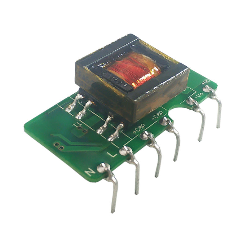
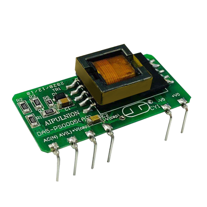
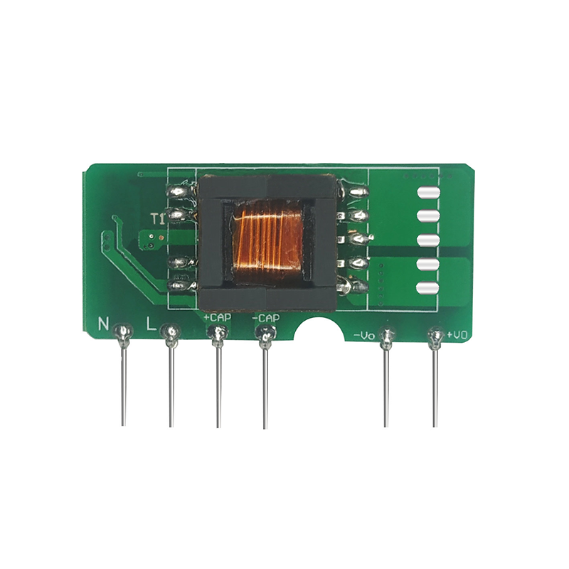


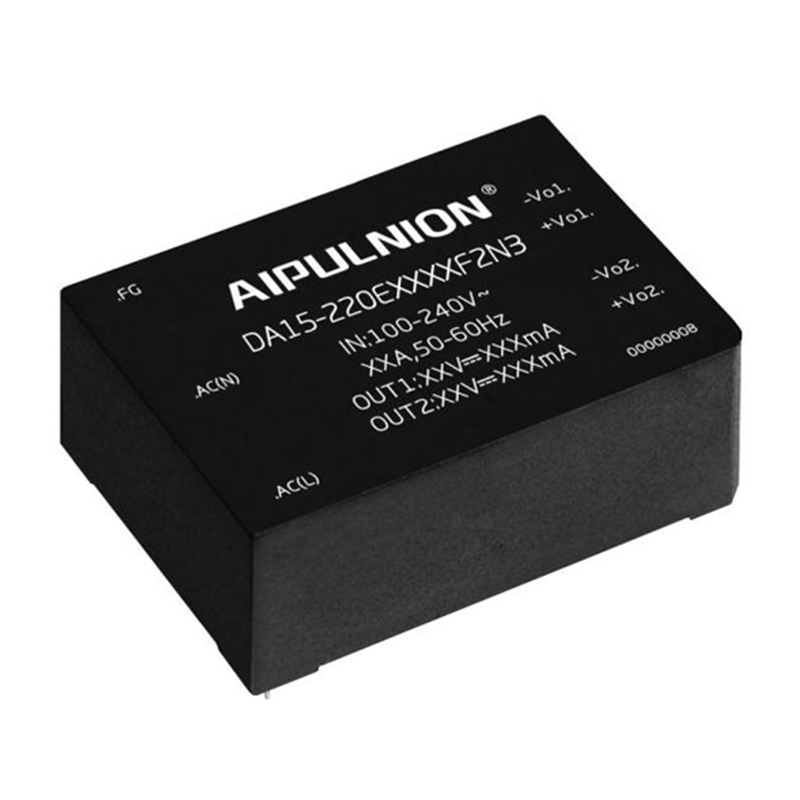


A Study of Diodes in Switching Power Supplies
lWhat is the difference between Schottky diodes and fast recovery diodes?
Fundamentally, Schottky diodes and fast recovery diodes are not the same in physical structure. The anode of Schottky diode is metal, the cathode is N-type semiconductor. The basic structure of the fast recovery diode is still an ordinary PIN diode, that is, the anode is N type semiconductors and the cathode is P type semiconductors. The physical structure determines the electrical properties of both.
1. The voltage resistance is low (usually below 150V). With the same voltage resistance and the same current, the forward voltage of the Schottky diode is lower than the fast recovery diode. According to the figure, when under 1A current, SS15 has a Vf of about 0.65V and ES1A has a Vf of 0.85V under 1A (both could withstand the same 50 voltage).


2. The Schottky diode carrier has only electrons. And the multi-digit device theoretically has no reverse recovery time. While the fast recovery diode is essentially the same as the PIN diode. And the reverse recovery time of the low-digit device is usually in the tens to hundreds of ns. What exactly is reverse recovery will be discussed in detail in Question 2 of Post 2.
3. Under the rated reverse voltage, the reverse leakage current of the fast recovery diode is small, usually in a few uA to dozens of uA. The reverse leakage current of Schottky diodes usually reaches hundreds of uA to tens of mA, and increases sharply with the increase of temperature.
l What is the reverse recovery time?
The basic definition of reverse recovery time is: the time required for the diode to transition from the on-state to the off state.
It can be seen from the definition that a reverse bias voltage is suddenly applied in the diode conduction state, and it cannot be cut off immediately. Let's figure out the reasons basically.

The picture above is the most basic structure of our most commonly used PN junction diode. The heavily doped P-type semiconductor acts as the anode and the heavily doped N-type semiconductor acts as the cathode. In order to withstand higher reverse voltage, there is a long region in the middle for the light doped N-type region close to the intrinsic semiconductor.
When PN junction is added with positive bias voltage, under the action of electric field, the holes in P region diffuse to N region, and the electrons in N region diffuse to P region, thus forming a forward current. For the P region, the electrons from the N region are minority. And for the N region, the holes from the P region are minority. Therefore, the PN junction diode actually transmits current through a small number of particles, that is, a small number of particles device. It can be seen that when the positive pilot passes, there are a large number of electrons in the P region and a large number of holes in the N region. The following take CCM's boost as an example, combined with simulation to analyze the diode reverse recovery problem.

The simulation results of the next steady state cycle are shown below:

V002 is the Vgs of the MOSFET. V(N003,N002) is the Vka of the diode. Id (M1) is the drain current of the MOSFET, and I (D1) is the anode inflow current of the diode.
When the new switching cycle comes, the MOSFET drive voltage rises. The inductive current begins to flow from the MOSFET, because the inductive current is basically unchanged in a short time. The current that the diode begins to flow begins to decrease. The moment the diode current decreases to 0 is the moment when reverse recovery begins.
Due to the few minority stored in the diode, the diode cannot block the current. As the MOSFET drive voltage rises, the loop impedance between MOSFET DS decreases. And the diode begins to reverse the current flow, that is, the form of the minority and reverse phase current is extracted until the voltage between MOSFET DS begins to drop (begins to enter the Miller platform). That is, when the diode starting voltage begins to reverse bias, the reverse current reaches the maximum value. After that, the reverse current begins to decrease and the diode reverse voltage begins to increase until the MOSFET Vds drops to 0. And the diode withstands the full reverse voltage.
It can be seen from the simulation diagram that in the process of reverse recovery, the diode flows through a large reverse current and bears a large reverse voltage, so a large reverse recovery loss is caused. In CCM PFCS, in order to reduce the loss, the usual ultra-fast recovery diode (nominal reverse recovery time of ten to tens of ns) is still unsatisfactory, and the SiC diode is needed. The commonly used SiC diodes are usually Schottky structures, and the reverse recovery time is much lower than that of PIN diodes.
l Is the diode power consumption an average current or an effective current?
The answer is average current. (The subject being discussed is the on-state loss of diode. And the reverse recovery loss is not considered.) Why is that?
First of all, the basic characteristic of the diode is a single direction channel, so the current is one-way (do not consider reverse recovery), and the diode on-voltage drop is generally considered to be basically unchanged. Obviously, the product of the current and voltage within a certain time, the result is the product of the average current and forward voltage drop, that is, the diode on-state loss is calculated by the average current.
Is the effective current meaningless? Not really. In addition to the PN junction, the diode also has the contact resistance and lead resistance of the package. The loss of these parts is evaluated by the effective value. But relative to the junction voltage drop, the voltage drop brought by the package can be ignored in most cases.
l Why some diode temperature is 150℃, some 175℃, some 125℃? What are the differences?
The maximum operating temperature is determined more by the packaging material and the packaging process than by the semiconductor itself. For Si materials, 175 degrees is usually no problem. Temperature resistance of SiC and GaN are higher. The same voltage resistance, the same current diode, the wafer area PIN occupy is much smaller than the Schottky diode.
About the voltage resistance of diodes:
Schottky's voltage is usually up to 200V (Taiwan Zhumao and PFC brands said it could be 300V, and the VF value could be 0.3). In fact, the reverse recovery time of Schottky is fast because its chip is very thin (the current is related to the size of the wafer area, and the voltage is related to the thickness of the wafer), and the distance between A and B is short. The ultra-fast recovery (SF,MUR,ER series) can withstand 600V, and the fast recovery (FR,HER,RS series) can withstand 1000V.
The maximum voltage of Schottky could be higher than 200V. But the silicon material restricts it. When the voltage is above 200V, Vf has no advantage relative to fast recovery. And the reverse leakage current is very large. A Schottky diode that can withstand 300V and Vf 0.3V has not been heard of and is theoretically unlikely. Schottky has no reverse recovery because the carriers are all electrons and there is no time to extract the minority.
l What is the forward current rating of the diode?
The rated current of the diode is the main nominal value of the diode. Take 5A/100V diode as an example, 5A is the rated current. The rated current is usually defined as the average rated current through which the diode can pass. However, some tests are preceded by square waves, that is, square-wave currents that can pass an average of 5A. Some tests are based on DC. In theory, for silicon diodes, the diode with square wave as the test condition can pass through a larger DC current. Because the square wave of the same average current will bring more losses to the diode than the DC current. Is the diode of 5A able to pass through the current of 5A? Not necessarily. This is related to temperature. When your heat dissipation conditions are not good enough, the current that the diode can pass through will be limited by the junction temperature.
l What is the reverse voltage rating of the diode?
When the diode is reversed, it can withstand a certain amount of back pressure. The highest back pressure it can withstand is the rated voltage. For example, 5A/100V diode, its rated back voltage is 100V. Although, all diode manufacturers will leave a certain margin. 100V diodes usually use 110V will not have a problem. However, it is not recommended. Because more than the rated value, the manufacturer will not guarantee its reliability. And many power supply design companies, in order to ensure reliability, will also reduce the rated value.
l What is the forward impulse current of the diode?
When switching power supply in running state or in other transient situation, the diode needs to be able to withstand a large impact current. Certainly, this impact current should be not repetitive.And the interval should not be too long. The impulse current is usually defined in the data manual of the diode. And the test condition is often a single waveform of the impulse current, such as a single sine wave, or square wave. Its current value could be up to several hundred.
l What is the positive pilot voltage drop of the diode?
When the diode works, it creates a voltage drop. This voltage drop is related to the forward current and temperature. As for silicon diodes, the greater the current, the greater the voltage drop. The higher the temperature, the lower the pressure drop. However, the higher the temperature of the silicon carbide diode, the greater the pressure drop.
l What is the reverse leakage current of the diode?
When the diode is reversed, it is not a completely ideal cutoff. When it is subjected to reverse voltage, some small current will leak from the cathode to the anode. This current is usually small. However, the higher the back voltage, the greater the leakage current. And the higher the temperature, the greater the leakage current. Large leakage current will bring large losses, especially in high voltage applications.
l What is the reverse recovery time and reverse recovery current of diodes?
This is an important indicator of the diode. Fast or slow is based on the following standard. When the diode is converted from positive bias to reverse bias, a large reverse recovery current will flow from the cathode to the anode. And the reverse current will first rise to the peak and then fall to zero. The time of its rise and fall is the reverse recovery time. The peak current is the reverse recovery current. This can cause a lot of loss in high frequency applications. The reverse recovery time is positively correlated with the decline rate of the forward current when the diode is cut off. To solve this problem, one could use a diode with a faster recovery time or use the ZCS mode to turn off the diode.
When the switch converts from the on-state to the off-state, the diode or rectifier needs to first release the stored charge before the diode blocks the reverse current. This discharge time is called the reverse recovery time, during which the current flows through the diode in the reverse direction. That is, from the time when the positive pilot current is 0 to the time when it enters the full cutoff state.
The reverse recovery process is actually caused by the charge storage effect. And the reverse recovery time is the time required for the charge stored in the PN junction to be exhausted during the forward conduction. If a continuous PWM wave with frequency T1 passes through the diode, and when Trr < t1, the reversed diode could not blocked the PWM wave. And the switching effect cannot be achieved. Reverse recovery time of diode is provided by datasheet. The fast reverse recovery time enables the diode to quickly convert between on-state and off-state, which can obtain a higher switching speed, increasing the usage frequency of the device and improve the waveform.
Fast recovery diode features
The most important feature of the fast recovery diode is that its reverse recovery time (trr) is below a few hundred nanoseconds (ns), and the ultra-fast recovery diode can even reach tens of nanoseconds. The reverse recovery time (trr) is defined as a time interval (current through the zero from the forward to reverse conversion, and then from the reverse conversion to the specified low value). It is an important technical index to measure the performance of high-frequency continuous current and rectifier devices.

In the figure, IF is the forward current. IRM is the maximum reverse recovery current. And Irr is the reverse recovery current. Generally, Irr=0.1IRM. When t≤t0, the forward current I=IF. When t > t0, because the forward voltage on the rectifier tube suddenly becomes the reverse voltage, the forward current rapidly decreases. And at the time t=t1, I=0. Then the reverse current IR on the rectifier tube increases gradually. The maximum reverse recovery current IRM value is reached at t=t2. After that, under the action of forward voltage, the reverse current gradually decreases and reaches the specified value Irr when t=t3. The reverse recovery process from t2 to t3 is similar to the discharge process of a capacitor. The interval from t1 to t3 is the reverse recovery time trr.
l What is a soft recovery diode?
When the diode recovers in reverse, the reverse current drops relatively slowly, which is called the soft recovery diode. Soft recovery has some advantages in reducing EMI.
l What is the junction capacitance of a diode?
The junction capacitance is a parasitic parameter of the diode and can be regarded as a capacitor in parallel on the diode.
l What is the parasitic inductance of diode?
The parasitic inductance of the diode is mainly caused by the lead and can be regarded as the inductance in series on the diode.
l What is the transient process when the electrode is positive?
For the transient process of diodes, the reverse recovery characteristic is usually the focus. However, in fact, the process of the diode from the reverse deflection to the positive pilot also has noteworthy aspects. When the diode switches on, the forward voltage drop will first rise to a maximum value, and then it will drop to the steady state value. And this maximum value increases as di/dt increases. That is to say, the diode band will generate a positive peak voltage at the moment of conduction. And the voltage is greater than the steady state voltage. The forward peak voltage of the fast recovery tube is relatively small, but the slow recovery tube is huge. Which brings us to another question.
l In the RCD clamp circuit, we should choose a slow tube or a fast tube?
RCD circuits are often used in situations where clamping is required, such as voltage clamping for flyback primary MOS and voltage clamping for secondary rectifier tubes. Some technical literature says that a slow recovery tube should be used, because the slow recovery tube has a long reverse recovery time, so that part of the energy in the clamp capacitor will be fed back to the circuit during the reverse recovery of the diode. And the loss of the entire RCD circuit can be reduced. But this is only suitable for small current or low di/dt like the low-power flyback’s primary side clamping circuit. However, it is not suitable for high-current, high-DI /dt clamping, such as the secondary clamping circuit of the power supply with a large current output. Because the slow recovery tube will produce a high on-voltage drop spike when it is on, resulting in a low voltage on the clamping capacitor, but it is unable to clamp the peak voltage. So we should choose something like a Schottky diode.
l What is silicon carbide diode?
Usually, silicon is used as raw material of the diodes, but recently the more popular raw materials
Is silicon carbide. At present, the most common high-voltage Schottky silicon carbide diodes have the advantages of good reverse recovery characteristics, comparable to Schottky silicon diodes. However, diodes that can do high voltage have many applications in PFC. And its disadvantage is that the forward guide pass pressure drop is relatively large. Another difference with silicon diodes is that their on-pressure drop increases with temperature. The early silicon carbide diodes also have the disadvantages of small impulse current and low reliability. But there has been great improvement.
l What is GaAs (gallium arsenide) diode?
To be honest, I heard that gallium arsenide material was earlier than silicon carbide. But later I heard less about it. At present, gallium arsenide seems to have some applications in LED, but it is still relatively small on power devices.
l Diodes suitable for parallel connection?
Theoretically speaking, silicon diodes, because the on-voltage drop decreases with the temperature rise, are not suitable for parallel connection. But now many diodes will package two single tubes together, so that the temperature rise is relatively uniform, which brings benefits to parallel connection. However, the pressure drop of silicon carbide is increased with the rise of temperature. So it is theoretically suitable for parallel operation.