


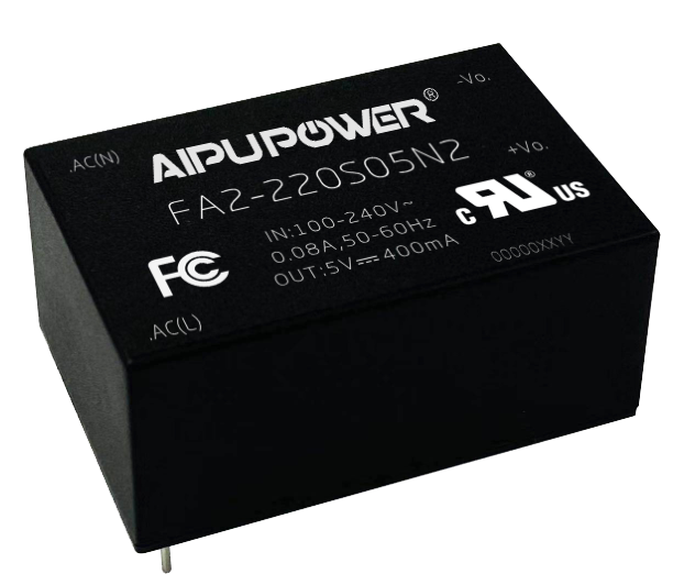
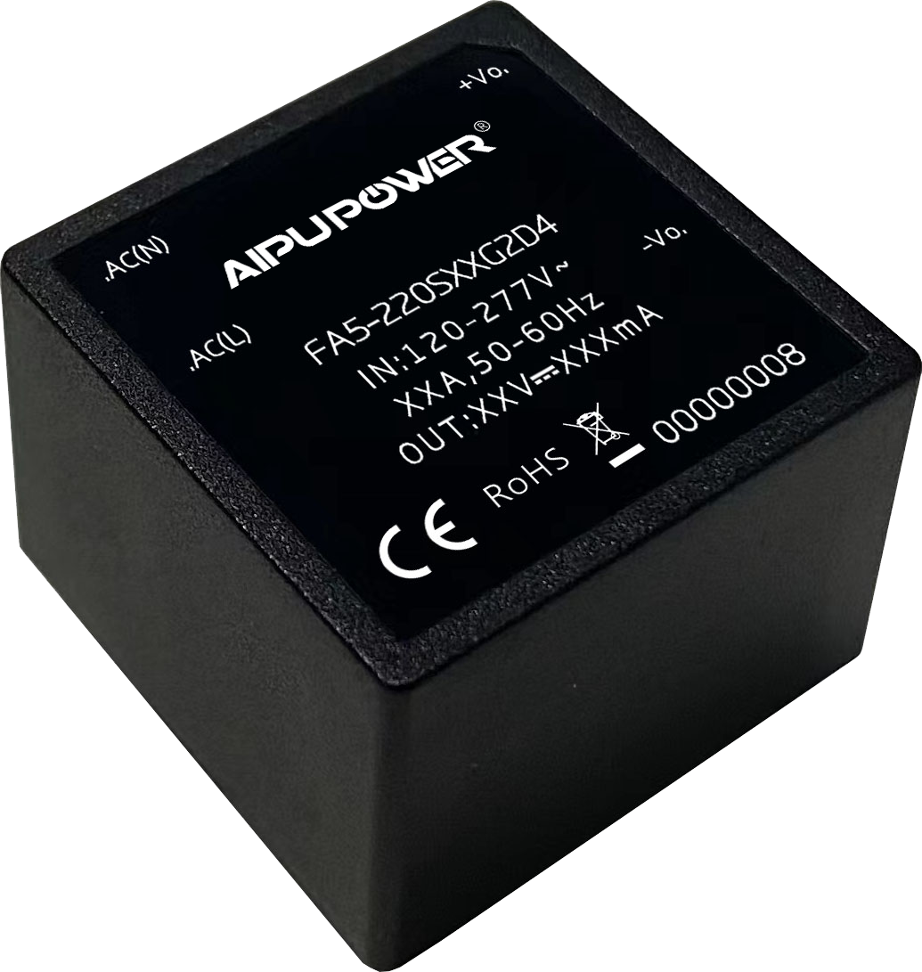


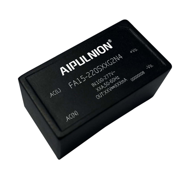


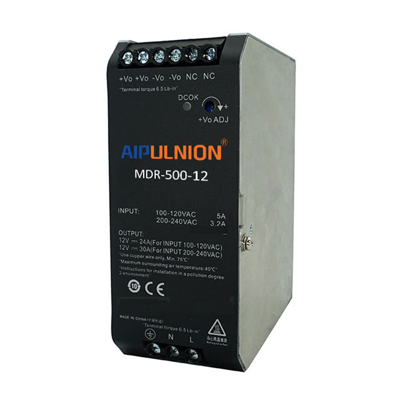


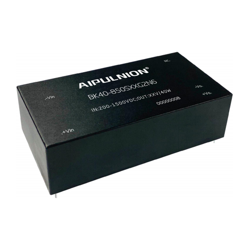


Layout and Design Principles of Switching Power Supply
Switching power supply works in high frequency and high pulse state, which is a special type of analog circuit. High frequency circuit wiring principles must be followed when laying out the board. After years of experience in the power supply industry, what new skills have you learned?
layout:
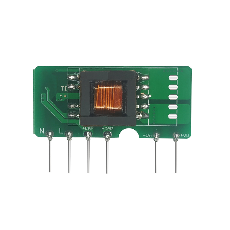
The pulse voltage connection should be as short as possible, including the connection between the input switch tube and the transformer and the connection between the output transformer and the rectifier tube. The pulse current loop should be as small as possible, such as the positive input filter capacitance to the negative return capacitance of the transformer to the switching tube. The X capacitor in the circuit from the output end of the transformer to the rectifier tube to the output inductor to the output capacitor returning to the transformer should be as close as possible to the input end of the switching power supply. The input line should not be parallel to other circuits and should be avoided. The Y capacitor should be placed at the chassis ground terminal or FG connection. Keep a certain distance between the common inductor and the transformer to avoid magnetic coupling. If it is difficult to handle, you can add a shield between the common inductor and the transformer. The above items have a greater impact on the EMC performance of the switching power supply.
Generally, two output capacitors can be used, one close to the rectifier and the other close to the output terminal, which can affect the power output ripple index. The effect of two small-capacity capacitors in parallel should be better than using one large-capacity capacitor. Heating devices should be kept at a certain distance from electrolytic capacitors to extend the life of the whole machine. Electrolytic capacitors are the bottleneck of the life of switching power supplies. For example, transformers, power tubes, and high-power resistors should be kept at a distance from electrolytic capacitors, and space for heat dissipation must also be left between electrolytic capacitors. , it can be placed at the air inlet if conditions permit.
Pay attention to the control part: the high-impedance weak signal circuit connections should be as short as possible, such as the sampling feedback loop, and try to avoid interference during processing. Current sampling signal circuits, especially current control circuits, may be prone to unexpected events if they are not handled well. Unexpectedly, there are some tricks. Now take the 3843 circuit as an example as shown in Figure (1). The effect of Figure 1 is better than Figure 2. In Figure 2, when using an oscilloscope to observe the current waveform at full load, there are obvious spikes superimposed on it. Due to the interference, the current limit point is larger than the design value. On the low side, there is no such phenomenon in Figure 1. There is also a switch tube drive signal circuit. The switch tube drive resistor should be close to the switch tube, which can improve the working reliability of the switch tube. This is related to the high DC impedance voltage drive characteristics of the power MOSFET.
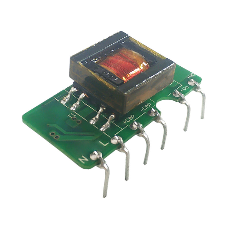
Switching power supply: layout and design principles, what new skills do you have?
Let’s talk about some principles of printed board wiring.
Line spacing: With the continuous improvement and improvement of printed circuit board manufacturing technology, there is no problem in general processing plants producing line spacing equal to or even less than 0.1mm, which can fully meet most applications. Considering the components and production process used in the switching power supply, generally the minimum line spacing of double-sided panels is set to 0.3mm, and the minimum line spacing of single-sided panels is set to 0.5mm. Pads and pads, pads and vias, or vias and vias holes, the minimum spacing is set to 0.5mm to avoid "bridging" during the welding operation. , so that most board manufacturers can easily meet production requirements, control the yield to a very high level, and achieve reasonable wiring density and a more economical cost.
The minimum line spacing is only suitable for signal control circuits and low-voltage circuits with voltages lower than 63V. When the voltage between lines is greater than this value, the line spacing can generally be determined based on the empirical value of 500V/1mm.
Since some relevant standards have clear regulations on line spacing, the standards must be strictly followed, such as the connection from the AC inlet end to the fuse end. Some power supplies have very high volume requirements, such as module power supplies. Generally, the spacing between the input side lines of a transformer is 1mm, which has been proven feasible in practice. For power products with AC input and (isolated) DC output, the strict requirement is that the safety distance must be greater than or equal to 6mm. Of course, this is determined by relevant standards and implementation methods. Generally, the safe distance can be used as a reference by the distance on both sides of the feedback optocoupler, and the principle is greater than or equal to this distance. Slots can also be made on the printed board below the optocoupler to increase the creepage distance to meet the insulation requirements. Generally, the distance between the AC input side traces or components on the switching power supply and the non-insulated shell or radiator should be greater than 5mm, and the distance between the output side traces or components and the shell or radiator should be greater than 2mm, or strictly follow safety regulations.
Commonly used methods: The circuit board slotting method mentioned above is suitable for some occasions where the spacing is insufficient. By the way, this method is also commonly used as a protective discharge gap. It is commonly used in TV picture tube tail plates and power supply AC inputs. . This method has been widely used in module power supplies and can achieve good results under potting conditions.
Method 2: Use insulating paper, such as green shell paper, polyester film, polytetrafluoroethylene directional film and other insulating materials. Generally, green paper or polyester film is used for general-purpose power supplies between the circuit board and the metal casing. This material has high mechanical strength and a certain ability to resist moisture. PTFE oriented film is widely used in module power supplies due to its high temperature resistance. An insulating film can also be placed between the component and surrounding conductors to improve the electrical resistance of the insulation.
Note: The insulation coating of some devices cannot be used as an insulating medium to reduce the safe distance, such as the outer skin of an electrolytic capacitor. Under high temperature conditions, the outer skin may shrink due to heat. Space should be left at the front of the large electrolytic explosion-proof tank to ensure that the electrolytic capacitor can relieve pressure without hindrance in emergency situations.
Let’s talk about some matters about printed circuit board copper wiring:
Wiring current density: Most electronic circuits are now made of insulating boards bound with copper. The commonly used circuit board copper thickness is 35μm, and the current density value for wiring can be determined based on the empirical value of 1A/mm. For specific calculations, please refer to the textbook. In order to ensure the mechanical strength of the wiring, the line width should be greater than or equal to 0.3mm (other non-power circuit boards may have a smaller minimum line width). Circuit boards with a copper thickness of 70μm are also common in switching power supplies, so the current density can be higher.
In addition, commonly used circuit board design tool software generally has design specification items, such as line width, line spacing, dry plate via size and other parameters that can be set. When designing circuit boards, the design software can automatically execute according to specifications, which can save a lot of time, reduce part of the workload, and reduce the error rate.
Generally, double-sided panels can be used for lines with high reliability requirements or high wiring density. It is characterized by moderate cost, high reliability, and can meet most applications.
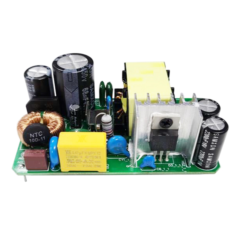
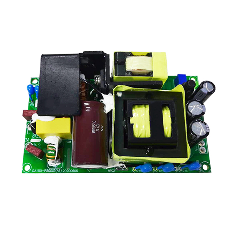
Some products in the modular power supply industry also use multi-layer boards, which are mainly used to facilitate the integration of power devices such as transformers and inductors, and to optimize wiring and power tube heat dissipation. It has the advantages of beautiful and consistent process and good heat dissipation of the transformer, but its disadvantages are higher cost and poor flexibility, and it is only suitable for industrial mass production.
Single-sided circuit boards are almost all common switching power supplies circulating in the market. They have the advantage of low cost, and some measures can be taken in the design and production process to ensure their performance.
Let’s talk about some experiences in the design of single-sided printed boards. Since single-sided boards are low-cost and easy to manufacture, they are widely used in switching power supply circuits. Since they have only one side with copper, the electrical connection and mechanical fixation of the device must rely on That layer of copper must be handled with care.
In order to ensure good welding mechanical structural performance, the single-sided pad should be slightly larger to ensure good bonding force between the copper and the substrate, so as to prevent the copper from peeling off or breaking off when subjected to vibration. Generally, the width of the welding ring should be greater than 0.3mm. The diameter of the pad hole should be slightly larger than the diameter of the device pin, but not too large to ensure that the solder connection distance between the pin and the pad is the shortest. The size of the pad hole should not hinder normal inspection. The diameter of the pad hole is generally larger than the pin. Diameter 0.1-0.2mm. Multi-pin devices can also be larger to ensure smooth inspection.
The electrical connection should be as wide as possible. In principle, the width should be greater than the diameter of the pad. In special cases, the line must be widened when the connection intersects with the pad (commonly known as teardrops) to avoid breakage of the line and the pad under certain conditions. In principle, the minimum line width should be greater than 0.5mm.
The components on the single panel should be close to the circuit board. For devices that require overhead heat dissipation, sleeves should be added to the pins between the device and the circuit board, which can play a dual role of supporting the device and increasing insulation. It is necessary to minimize or avoid external force impact on the connection between the pad and the pins. The impact caused by the welding enhances the firmness of the welding. For heavier components on the circuit board, support connection points can be added to strengthen the connection strength with the circuit board, such as transformers and power device radiators.
The pins on the soldering surface of a single panel can be left longer without affecting the distance from the shell. The advantage is that it can increase the strength of the welding part, increase the welding area, and detect any weak soldering immediately. When the pins are long and the legs are cut, the stress on the welding part is smaller. In Taiwan and Japan, the process of bending the device pins on the soldering surface to an angle of 45 degrees with the circuit board and then soldering is often used. The principle is the same as above. Today we will talk about some issues in double-sided PCB design. In some application environments with relatively high requirements or high wiring density, the performance and various indicators of double-sided PCBs are much better than those of single-sided PCBs.
The double-sided pad has higher strength because the holes have been metallized, so the soldering ring can be smaller than that of a single-sided board, and the pad hole diameter can be slightly larger than the pin diameter, because during the welding process it is helpful for the solder solution to penetrate into the top layer through the welding holes. pad to increase soldering reliability. But there is a drawback. If the hole is too large, some components may float up under the impact of jet tin during wave soldering, causing some defects.
When dealing with high-current traces, the line width can be processed according to the previous post. If the width is not enough, it can generally be solved by tin plating on the traces to increase the thickness. There are many methods:
1. Set the trace to the pad attribute so that the trace will not be covered by solder resist during circuit board manufacturing and will be tinned during hot air leveling.
2. Place the pad at the wiring location and set the pad into the shape required for routing. Be careful to set the pad hole to zero.
3. Place lines on the solder mask layer. This method is the most flexible, but not all circuit board manufacturers will understand your intention, so you need to explain it in words. No solder resist will be applied where the solder mask lines are placed.
Several methods of tin plating circuits are as follows. It should be noted that if very wide traces are all tinned, a large amount of solder will be adhered after welding, and the distribution will be very uneven, affecting the appearance. Generally, slender tinned strips with a width of 1~1.5mm can be used, and the length can be determined according to the line. The tinned parts are spaced 0.5~1mm apart. Double-sided circuit boards provide great selectivity for layout and wiring, making wiring more efficient. tend to be reasonable. Regarding grounding, the power ground and signal ground must be separated. The two grounds can be combined at the filter capacitor to avoid unexpected unstable factors caused by large pulse currents passing through the signal ground connection. Try to use a one-point grounding method for the signal control loop. There is a trick, try to place the non-grounded traces on the same wiring layer, and finally lay the ground wire on another layer. The output line generally passes through the filter capacitor first, and then to the load. The input line must also pass through the capacitor first, and then to the transformer. The theoretical basis is to let the ripple current pass through the filter capacitor.
Voltage feedback sampling, in order to avoid the influence of large current passing through the wiring, the sampling point of the feedback voltage must be placed at the end of the power supply output to improve the load effect index of the whole machine.
The change of wiring from one wiring layer to another is generally connected through via holes. It should not be realized through the device pin pads, because this connection relationship may be destroyed when the device is inserted, and when every 1A current passes, There should be at least 2 via holes. The diameter of the via holes should be greater than 0.5mm in principle. Generally, 0.8mm can ensure processing reliability.
Device heat dissipation. In some low-power power supplies, the circuit board traces can also serve as heat dissipation functions. The characteristic is that the traces are as wide as possible to increase the heat dissipation area. Solder resist is not applied. If possible, vias can be evenly placed to enhance thermal conductivity. .
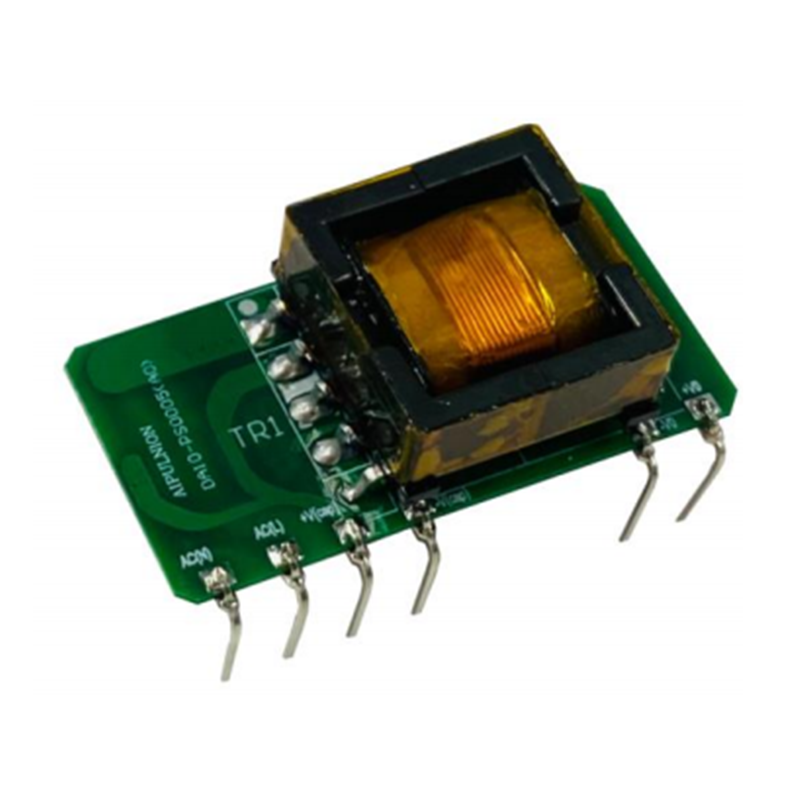
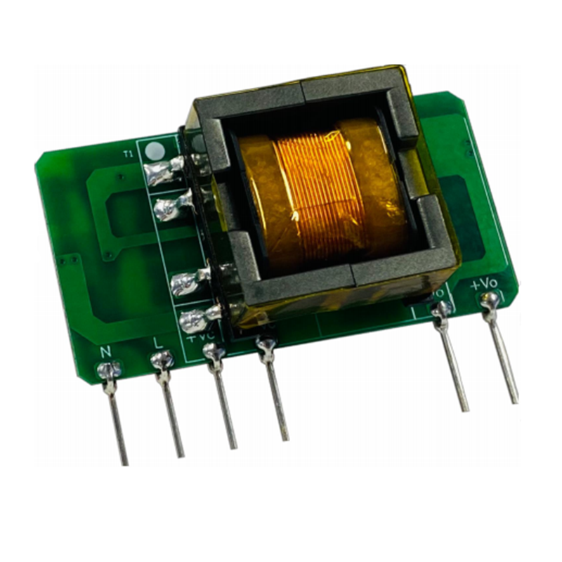
Let’s talk about the application of aluminum substrates in switching power supplies and the application of multi-layer printed boards in switching power supply circuits.
The aluminum substrate is constructed by itself and has the following characteristics: very good thermal conductivity, copper bonding on one side, devices can only be placed on the copper bonding surface, and electrical wiring holes cannot be opened, so jumpers cannot be placed like single panels.
SMD devices, switching tubes, and output rectifier tubes are generally placed on the aluminum substrate to conduct heat out through the substrate. The thermal resistance is very low and high reliability can be achieved. The transformer adopts a planar patch structure and can also dissipate heat through the substrate. Its temperature rise is lower than conventional ones. Transformers with the same specifications using an aluminum substrate structure can obtain greater output power. Aluminum substrate jumpers can be handled by bridging. Aluminum substrate power supply generally consists of two printed boards, the other board houses the control circuit, and the two boards are integrated through physical connection.
Due to the excellent thermal conductivity of the aluminum substrate, it is more difficult to manually weld in small quantities. The solder cools too quickly, which is prone to problems. There is a simple and practical method. Use an ordinary electric iron (preferably with a temperature adjustment function) for ironing clothes. Turn it over, ironing side up, fix it, adjust the temperature to about 150°C, put the aluminum substrate on the iron, heat it for a period of time, then attach and solder the components according to the conventional method. The temperature of the iron should be such that the device is easy to solder. , if the temperature is too high, the device may be damaged, or even the copper sheet of the aluminum substrate may peel off. If the temperature is too low, the welding effect will be poor, so it must be controlled flexibly.
In recent years, with the application of multi-layer circuit boards in switching power supply circuits, it has become possible to print circuit transformers. Due to the small layer spacing of multi-layer boards, the transformer window cross-section can also be fully utilized, and additional circuit boards can be added to the main circuit board. Add one or two printed coils composed of multi-layer boards to utilize the window and reduce the line current density. Due to the use of printed coils, manual intervention is reduced. The transformer has good consistency, planar structure, low leakage inductance, and good coupling. . Open magnetic core, good heat dissipation conditions. Because it has many advantages and is conducive to mass production, it has been widely used. However, the initial investment in research and development is relatively large and is not suitable for small-scale production.
Switching power supplies are divided into two forms: isolated and non-isolated. Here we mainly talk about the topological form of isolated switching power supplies. In the following, unless otherwise specified, all refer to isolated power supplies. Isolated power supplies can be divided into two categories according to different structural forms: forward type and flyback type. Flyback means that when the primary side of the transformer is turned on, the secondary side is turned off and the transformer stores energy. When the primary side is cut off, the secondary side is turned on, and the energy is released to the working state of the load. Generally, there are many conventional flyback power supplies with single tubes, and double tubes are uncommon. Forward type means that when the primary side of the transformer is turned on, the secondary side induces a corresponding voltage and outputs it to the load, and the energy is transferred directly through the transformer.According to specifications, it can be divided into conventional forward, including single-tube forward and double-tube forward. Both half-bridge and bridge circuits are forward circuits.
Forward and flyback circuits each have their own characteristics, which can be used flexibly in order to achieve optimal cost performance during circuit design. Generally, flyback type can be used in low-power situations. For slightly larger ones, a single-tube forward circuit can be used, for medium power, a two-tube forward circuit or a half-bridge circuit can be used, and for low voltage, a push-pull circuit can be used, which is the same as the half-bridge working state. For high-power output, a bridge circuit is generally used, and a push-pull circuit can also be used for low voltage.
Flyback power supplies are widely used in small and medium-power power supplies because of their simple structure and the elimination of an inductor that is about the same size as a transformer. In some introductions, it is said that the power of flyback power supply can only reach tens of watts. If the output power exceeds 100 watts, there is no advantage and it is difficult to implement. I think this is generally the case, but it cannot be generalized. PI's TOP chip can achieve 300 watts. There are articles saying that flyback power supplies can achieve kilowatts, but I have never seen a real one. The output power is related to the output voltage.
The leakage inductance of the flyback power supply transformer is a very critical parameter. Since the flyback power supply requires the transformer to store energy, in order to fully utilize the transformer core, an air gap must be opened in the magnetic circuit. The purpose is to change the core hysteresis. The slope of the loop enables the transformer to withstand large pulse current impacts without causing the core to enter a saturated non-linear state. The air gap in the magnetic circuit is in a high reluctance state, and the magnetic leakage generated in the magnetic circuit is much greater than that of a completely closed magnetic circuit. .
The coupling between the primary poles of the transformer is also a key factor in determining the leakage inductance. To keep the primary pole coils as close as possible, the sandwich winding method can be used, but this will increase the distributed capacitance of the transformer. When choosing an iron core, try to use a core with a longer window to reduce leakage inductance. For example, using EE, EF, EER, and PQ type cores has better effects than EI type.
Regarding the duty cycle of the flyback power supply, in principle, the maximum duty cycle of the flyback power supply should be less than 0.5, otherwise the loop will not be easily compensated and may be unstable. However, there are some exceptions. For example, the TOP series chips launched by the American PI Company are Can work under the condition that the duty cycle is greater than 0.5. The duty cycle is determined by the primary and secondary turns ratio of the transformer. My opinion on doing flyback is to first determine the reflected voltage (the voltage value at which the output voltage is reflected to the primary through transformer coupling). When the reflected voltage increases within a certain voltage range, The working duty cycle increases and the switching tube loss decreases. When the reflected voltage decreases, the operating duty cycle decreases and the switching tube loss increases. Of course, this also has prerequisites. When the duty cycle increases, it means that the output diode conduction time is shortened. In order to maintain output stability, it will be guaranteed by the output capacitor discharge current more often, and the output capacitor will withstand greater high frequency. Ripple current washes away and heats up, which is not allowed under many conditions. Increasing the duty cycle and changing the turns ratio of the transformer will increase the leakage inductance of the transformer and change its overall performance. When the leakage inductance energy reaches a certain level, it can fully offset the low loss caused by the large duty cycle of the switching tube. At this time, there is no point in increasing the duty cycle, and the switching tube may even be broken down because the leakage inductance reverse peak voltage is too high. Due to the large leakage inductance, the output ripple and other electromagnetic indicators may deteriorate. When the duty cycle is small, the effective value of the switching tube current is high, and the effective value of the transformer primary current is large, which reduces the efficiency of the converter, but can improve the working conditions of the output capacitor and reduce heat generation.
How to Determine Transformer Reflected Voltage (i.e. Duty Cycle)
Some netizens mentioned the parameter settings and working status analysis of the feedback loop of the switching power supply. Because I was relatively poor in advanced mathematics when I was in school, I almost took the make-up exam for "Principles of Automatic Control". I am still afraid of this subject. I still cannot fully write the transfer function of a closed-loop system, and I have a feeling for the concepts of zeros and poles of the system. It's very vague. Looking at the Bode plot, you can only roughly tell whether it is diverging or converging, so I don't dare to talk nonsense about feedback compensation, but I have some suggestions. If you have some mathematical skills and some study time, you can find the university textbook "Principles of Automatic Control" and digest it carefully, and analyze it according to the working status based on the actual switching power supply circuit. You will definitely gain something. There is a post on the forum "Apprenticeship to Learn Feedback Loop Design and Adjustment" where CMG gave a good answer. I think it can be used as a reference.
Next, let’s talk about the duty cycle of the flyback power supply (I focus on the reflected voltage, which is consistent with the duty cycle). The duty cycle is also related to the withstand voltage of the selector switch. Some early flyback power supplies use relatively low withstand voltage switch tubes. For example, 600V or 650V is used as a switching tube for AC 220V input power supply. This may be related to the production process at that time. High-voltage tubes are difficult to manufacture, or low-voltage tubes have more reasonable conduction losses and switching characteristics, such as line reflections. The voltage cannot be too high, otherwise in order to make the switching tube work within a safe range, the power absorbed by the circuit loss is also considerable. Practice has proved that the reflected voltage of a 600V tube should not be greater than 100V, and the reflected voltage of a 650V tube should not be greater than 120V. When the leakage inductance peak voltage value is clamped to 50V, the tube still has a working margin of 50V. Nowadays, due to the improvement of MOS tube manufacturing technology, generally flyback power supplies use 700V or 750V or even 800-900V switching tubes. For a circuit like this, the switching transformer's reflection voltage can be made higher because it has a stronger ability to withstand overvoltage. The maximum reflection voltage is 150V, which is more appropriate and can achieve better overall performance. PI's TOP chip recommends using transient voltage suppression diode clamps for 135V. However, the reflected voltage of his evaluation board is generally lower than this value, around 110V. Both types have advantages and disadvantages:
Category 1: Disadvantages: weak overvoltage resistance, small duty cycle, and large primary pulse current of the transformer. Advantages: The transformer has small leakage inductance, low electromagnetic radiation, high ripple index, small switching tube loss, and the conversion efficiency is not necessarily lower than the second type.
Category 2: Disadvantages: The switching tube loss is larger, the transformer leakage inductance is larger, and the ripple is worse. Advantages: stronger overvoltage resistance, large duty cycle, lower transformer loss, and higher efficiency.
There is another determining factor for the reflected voltage of the flyback power supply.
The reflected voltage of the flyback power supply is also related to one parameter, that is, the output voltage. The lower the output voltage, the greater the turns ratio of the transformer, the greater the leakage inductance of the transformer, and the higher the voltage the switch tube can withstand, which may cause breakdown of the switch tube and absorb the voltage. The greater the power consumed by the circuit, the more likely it is that the circuit power absorption device will permanently fail (especially circuits using transient voltage suppression diodes). Care must be taken in the optimization process of designing a low-voltage output low-power flyback power supply. There are several ways to do this:
1. Use a magnetic core with a larger power level to reduce leakage inductance, which can improve the conversion efficiency of low-voltage flyback power supplies, reduce losses, reduce output ripple, and improve the cross-regulation rate of multi-channel output power supplies. It is generally common in switches for home appliances. Power supply, such as CD player, DVB set-top box, etc.
2. If conditions do not allow increasing the magnetic core, the reflected voltage can only be reduced and the duty cycle reduced. Reducing the reflected voltage can reduce the leakage inductance but may reduce the power conversion efficiency. The two are contradictory. There must be a replacement process to find a suitable point. During the transformer replacement experiment, the primary side of the transformer can be detected. Reverse peak voltage, try to reduce the width and amplitude of the reverse peak voltage pulse, which can increase the operating safety margin of the converter. Generally, the reflected voltage is more suitable when it is 110V.
3. Enhance coupling, reduce losses, and adopt new technologies and winding processes. In order to meet safety regulations, the transformer will take insulation measures between the primary side and the secondary side, such as padding with insulating tape and adding insulating terminal tape. These will affect the leakage inductance performance of the transformer. In actual production, the primary winding can be used to wrap the secondary winding. Or the secondary is wound with triple insulated wire, eliminating the insulation between the primary and secondary, which can enhance the coupling, or even be wound with a wide copper sheet.
In this article, low-voltage output refers to an output less than or equal to 5V. For this type of low-power power supply, my experience is that if the power output is greater than 20W, the forward mode can be used to obtain the best cost performance. Of course, this is not absolutely correct. It depends on personal habits and application environment.
The magnetic core of the flyback power transformer works in a unidirectional magnetization state, so the magnetic circuit needs an air gap, similar to a pulsating DC inductor. Part of the magnetic circuit is coupled through the air gap. The principle of why the air gap is opened is as follows: Since power ferrite also has an approximately rectangular operating characteristic curve (hysteresis loop), the Y-axis on the operating characteristic curve represents the magnetic induction intensity (B). The current production process is generally The saturation point is above 400mT. Generally, this value should be 200-300mT in design. The X-axis represents the magnetic field intensity (H). This value is proportional to the magnetizing current intensity. Opening an air gap in the magnetic circuit is equivalent to tilting the magnet's hysteresis loop toward the X-axis. Under the same magnetic induction intensity, it can withstand a larger magnetizing current, which is equivalent to the magnetic core storing more energy. This energy is cut off at the switching tube. When it is discharged to the load circuit through the secondary side of the transformer, the air gap in the flyback power core has two functions. One is to transfer more energy, and the other is to prevent the core from entering saturation.
The transformer of the flyback power supply works in a unidirectional magnetization state. It not only transfers energy through magnetic coupling, but also plays the multiple roles of voltage conversion input and output isolation. Therefore, the handling of the air gap needs to be very careful. If the air gap is too large, the leakage inductance will increase, the hysteresis loss will increase, the iron loss and copper loss will increase, which will affect the overall performance of the power supply. An air gap that is too small may saturate the transformer core, causing damage to the power supply.
The so-called continuous and intermittent modes of flyback power supply refer to the working state of the transformer. In the full load state, the transformer works in the working mode of complete energy transfer or incomplete energy transfer. Generally, the design should be based on the working environment. Conventional flyback power supplies should work in continuous mode, so that the losses of switching tubes and circuits are relatively small, and the working stress of the input and output capacitors can be reduced. However, there are some exceptions. It needs to be pointed out here: due to the characteristics of the flyback power supply, it is more suitable to be designed as a high-voltage power supply, and high-voltage power transformers generally work in intermittent mode. I understand that the high-voltage power supply output requires the use of high-voltage rectifier diodes. Due to the characteristics of the manufacturing process, high reverse voltage diodes have long reverse recovery time and low speed. In the continuous current state, the diode recovers when there is forward bias. The energy loss during reverse recovery is very large, which is not conducive to the performance of the converter. The improvement will at least reduce the conversion efficiency, cause the rectifier tube to become seriously heated, and at worst, even burn the rectifier tube. Since in discontinuous mode, the diode is reverse biased at zero bias, the loss can be reduced to a relatively low level. Therefore, the high-voltage power supply operates in intermittent mode, and the operating frequency cannot be too high. There is also a type of flyback power supply that works in a critical state. Generally, this type of power supply works in frequency modulation mode, or frequency modulation and width modulation dual mode. Some low-cost self-excited power supplies (RCC) often use this form. In order to ensure output stability, the transformer The operating frequency changes with the output current or input voltage. When it is close to full load, the transformer always remains between continuous and intermittent. This kind of power supply is only suitable for low-power output, otherwise the electromagnetic compatibility characteristics will be a headache.
The flyback switching power supply transformer should work in continuous mode, which requires a relatively large winding inductance. Of course, there is also a certain degree of continuity. It is unrealistic to pursue absolute continuity excessively. It may require a large magnetic core, and a lot of The number of coil turns, along with large leakage inductance and distributed capacitance, may not be worth the trade-off. So how to determine this parameter? After many times of practice and analysis of peer designs, I believe that when the nominal voltage is input, it is more appropriate for the output to reach 50%~60% for the transformer to transition from intermittent to continuous state. Or in the highest input voltage state, at full load output, the transformer can transition to the continuous state.