


High-Performance Buck Regulator Addresses Power Dissipation Issues in Transmitter Circuits in Current Loops
The high-performance buck regulator is a cutting-edge technology that plays a crucial role in various electronic circuits. It is designed to efficiently step down the input voltage to a stable and regulated output voltage, addressing power consumption issues in a wide range of applications.
One of the key advantages of a high-performance buck regulator is its ability to minimize power loss. Traditional linear regulators dissipate excess voltage as heat, resulting in significant energy wastage. In contrast, the buck regulator utilizes a switching mechanism that converts the excess voltage into a lower output voltage with minimal power loss. This significantly improves the overall efficiency of the circuit and reduces power consumption.
In addition to its energy-saving capabilities, the high-performance buck regulator also offers excellent voltage regulation. It ensures a stable output voltage even in the presence of input voltage fluctuations or changes in load conditions. This is particularly important in sensitive electronic devices where a stable voltage is crucial for their proper functioning and longevity.
Furthermore, the high-performance buck regulator is highly versatile and can be used in a wide range of applications. It is commonly employed in power management systems, battery-powered devices, and communication circuits. Its compact size and high efficiency make it an ideal choice for portable electronic devices where power consumption and battery life are critical factors.
Moreover, the high-performance buck regulator is designed to handle high current loads, making it suitable for applications that require robust power delivery. It can efficiently regulate the voltage even in demanding situations, ensuring reliable and stable operation of the circuit.
In conclusion, the high-performance buck regulator is a groundbreaking technology that addresses power consumption issues in electronic circuits. Its efficient power conversion capabilities, excellent voltage regulation, and versatility make it an indispensable component in a wide range of applications. With its ability to minimize energy wastage and ensure stable voltage output, the high-performance buck regulator significantly enhances the overall performance and efficiency of electronic devices.
Automated controls are increasingly common in industrial and consumer applications, but even best-in-class automation solutions rely on an age-old technology: the current loop. Current loops are ubiquitous components in control loops that work in both directions: they pass measurements from sensors to programmable logic controllers (PLCs), and conversely, they pass control outputs from PLCs to process modulation devices.
The 4mA to 20mA current loop is the mainstream industry standard method for accurately and reliably transmitting data from remote sensors to PLCs over twisted pair wires. Simple, durable, robust, mature and reliable long-distance data transmission, good noise immunity and low installation costs make this interface ideal for long-term industrial process control and automatic monitoring of remote objects in noisy environments. Traditionally, power for the current loop has been provided through a linear regulator for many of the reasons mentioned earlier. The disadvantages of using linear regulators are relatively low efficiency and limited current capacity compared to switching regulators. Inefficiencies can lead to thermal issues, and limited current flow often prevents the addition of needed control system functionality.
New high-efficiency, high-input-voltage buck regulators are rugged and small enough to replace linear regulators in many current loop systems. Buck regulators have many advantages over linear regulators, including higher current capacity, wider input range, and higher system efficiency. Buck regulators offer clear performance advantages, with shorter tON times at high switching frequencies, helping to provide compact, stable solutions.
background knowledge
The standard 4mA to 20mA current loop shown in Figure 1 can be used to transmit sensor information and control signals from field instrumentation to process modulating devices, such as valve positioners or other output actuators. It consists of four parts:

Figure 1.2-wire current loop diagram
Current Loop Power Supply: The supply voltage VDC varies depending on the application (9VDC, 12VDC, 24VDC, etc.) and has a potential that is at least 10% higher than the voltage drop of the combined components in the circuit (such as transmitter, receiver, and wires). This VDC is tapped by a local buck regulator to power sensors and other components.
Transmitter: The main component of the transmitter is the sensor or transducer. It converts physical signals such as temperature, pressure, current, distance or magnetic field into electrical signals. If the converted signal is an analog voltage, a voltage-to-current converter is required as part of the transmitter to convert the voltage into a 4mA to 20mA current signal. For smart digital output sensors, the digital signal is converted back to an analog signal through a DAC. Local power supplies in the transmitter LDO or buck regulator power all of these analog, digital, and reference circuits.
Receiver or Monitor: A receiver converts a 4mA to 20mA current signal into a voltage signal that can be further processed and/or displayed. The current signal is converted to a useful voltage level through a high-precision shunt resistor RSHUNT and/or an analog-to-digital converter or data acquisition circuit. At the instrument terminals, a local buck regulator powers the receiver circuitry.
2-Wire or 4-Wire Loop: A complete current loop circuit can extend over 2000 feet and consists of a transmitter, power supply, and receiver in series. In a 2-wire 4mA to 20mA current loop, the power supply and current loop share the same loop.
For example, to measure pressure from 0psi to 50psi using a remote pressure sensor, a 4mA to 20mA current receiver circuit is in series with a pressure-to-current converter. On the sensor side, a pressure of 0psi reads 4mA, and a pressure of 50psi reads 20mA. At the receiver side, we know from Kirchhoff's first law that the same current appears across the shunt resistor and converts it into a voltage signal.
Automated operations in industrial, refinery, highway monitoring and consumer applications require high-performance sensor technology and reliable, accurate current loops to transmit sensor information. The components of the current loop must maintain high accuracy, low power consumption and reliable operation over the extended –40°C to +105°C industrial temperature range, as well as provide necessary safety and system functionality.
The supply voltage on the transmitter (sensor) side can be as high as 65V during transients and must be converted to 5V or 3.3V. Since sensor circuits are usually designed to draw power directly from the current loop (no additional local power supply), this is usually limited to 3.5mA. As transmitter features increase, this limitation becomes a problem when using a conventional linear regulator, which cannot supply any additional current. Additionally, in systems using linear regulators, most of the power must be dissipated in the regulator, creating a lot of heat in the packaged system.
The ADI LT8618, a 100mA high-speed synchronous monolithic step-down switching regulator, extends the input range to 65V and the load capability to 15mA. Its high efficiency eliminates thermal constraints in current loop system designs where the emitter is packaged and exposed to harsh environmental changes. It is recommended to use a low-cost filter to reduce the voltage ripple and the current ripple on the cable side. This article analyzes power regulator performance and provides component selection guidelines to meet stringent industrial requirements. In addition, test data such as efficiency, startup, and ripple are also provided.
Closing the current loop using a buck converter with extended input and load ranges
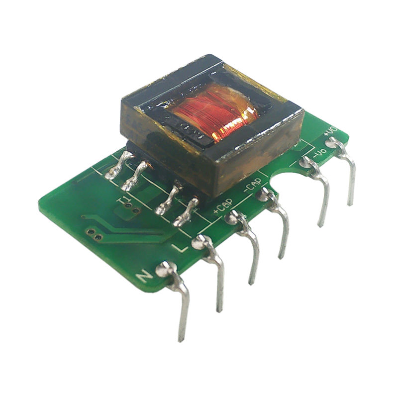
The LT8618 is a compact buck converter with numerous features to meet the requirements of industrial, automotive and other unpredictable power environments. It is ideally suited for 4mA to 20mA current loop applications, featuring ultra-low quiescent current, high efficiency, wide input range, voltages up to 65V and compact size. Figure 2 shows a complete transmitter circuit solution that uses the LT8618 to power the MAX6192C precision voltage reference, voltage-to-current conversion, and other circuitry.

Figure 2. Current loop using LT8618 as DC power supply
The current of the shunt circuit 2SC1623 is proportional to the voltage applied to the positive input of the error amplifier (EA). The 2.5V reference voltage is generated by the MAX6192C. The MAX6192C is a precision voltage reference IC that features low noise, low voltage drop, and low temperature drift of 5ppm/°C maximum. For smart sensors whose digital output is proportional to an environmental variable, a DAC can convert the digital signal to an analog signal and send it to an error amplifier.
Therefore, with the EA, BJT (2SC1623) and 100Ω (±0.1%) sense resistor (RSENSE), the converter modulates the current in the current loop from 4mA to 20mA, where 4mA represents a non-zero minimum output and 20mA represents the maximum signal . Even if the field transmitter does not have a process signal output, a non-zero minimum output of 4mA or an output above zero can power the device. Therefore, the current in the shunt circuit is proportional to environmental variables, such as pressure, temperature, level, flow, humidity, radiation, pH or other process variables.
The two long wires are part of the information carrying current loop and are also used to supply power to the transmitter from VDC (the power supply on the receiver side). The minimum voltage of VDC should be sufficient to cover the voltage drop between the conductors, shunts and the minimum operating voltage of the transmitter. The supply voltage depends on the application, usually 12V or 24V, but can be as high as 36V.
At the remote transmitter terminal, a Schottky diode (D1) protects the transmitter from reverse current. Placing a Zener diode or TVS (D2) diode at the input provides further protection, limiting transient voltage surges that are proportional to the current loop inductance. The LT8618 high-efficiency monolithic buck regulator reduces the loop voltage to 5.5V or 3.3V to power the reference, DAC, and other functional units.
In Figure 2, the wiring between VDC and transmitter can vary from a few feet to 2000 feet. The stray inductance of the current loop and the input capacitance of the buck regulator form an LC resonant tank. Transients on the power supply side (VDC) also occur on the input side of the remote transmitter. For worst-case undamped oscillation, the peak voltage may be twice VDC. For example, if the typical operating input voltage is 24V and the maximum specification is 36V, then the maximum voltage on the transmitter side may exceed 65V. As shown in Figure 2, protection can be easily implemented using TVS diode D2 in front of the transmitter to limit any surges during transients.
Alternatively, an efficient system can be built by using an LDO regulator to protect the LT8618 from high voltage excursions. In this topology, the LDO regulator will regulate to the input voltage minus its dropout voltage, while the LT8618 converts ~24V to 5V or 3.3V with high efficiency. The current limit of the LDO regulator should be set below the usual 3.8mA while maintaining high efficiency, and the input capacitor of the LT8618 basically uses decoupling capacitors and energy storage capacitors. This will support short bursts of high load on the backend with minimal or no current draw in the current loop. Because the high-voltage excursion is shorter and typically carries less total energy, the power losses incurred in the LDO regulator during these transients do not affect overall efficiency; that is, the LDO regulator is in the Under high voltage reduction ratio.
A typical current loop limits the input current to the power circuit that powers the entire remote transmitter, and the LDO regulator's available load current cannot exceed this input current limit. On the other hand, a buck regulator can multiply the input current supplied to the load. Figure 3 shows the output current versus input current of the LT8618 regulator when converting from a 24V input voltage to a 5.5V output. For an input current limit of 3.8mA, the output current is almost 15mA. This additional power increases operating margin and enables additional functional units, simplifying the system designer's work.

Figure 3. Output current vs. input current, VIN = 24V, VOUT = 5.5V
Burst mode operation improves efficiency at light loads
The efficiency of the LDO regulator is proportional to the step-down ratio (VOUT/VIN). When the input voltage is slightly higher than the output voltage, the efficiency will be very high. Problems will occur when the voltage reduction ratio is too high, in which the efficiency is very low and will cause great thermal stress to the system. For example, when the input voltage is 55V and the output voltage is 3.3V, the power loss of the LDO regulator is 0.19W and the load current is 3.8mA. In contrast, a properly designed buck regulator can be very efficient at a high step-down ratio. In addition, compared with non-synchronous regulators, synchronous buck regulators can replace the freewheeling diodes with MOSFETs, thereby improving efficiency. The challenge with synchronous buck converters is to optimize efficiency over the entire load range, especially at light loads of 3mA to 15mA, where the input voltage can be as high as 65V.
For a typical synchronous buck converter, there are three main power losses: switching losses, gate drive losses, and losses associated with the converter IC controller logic. If you reduce the switching frequency, you can greatly reduce the switching and gate drive losses, so you can reduce the switching and gate losses at light loads simply by running the converter at a low frequency.
At light loads, the bias losses of logic circuits are comparable to the relatively low switch-related losses. The bias circuit is normally powered from the output and draws power from the input through the internal LDO regulator only during startup and other transient conditions.
At light load, the LT8618 solves the problem of logic circuit loss by running Burst Mode®. At this time, the current is delivered to the output capacitor in the form of short pulses, and then enters a relatively long sleep period, during which most of the logic control circuitry is turned off.
To improve light load efficiency, a larger value inductor can be used because more energy can be transferred to the output during short switching pulses and the buck regulator can remain in sleep mode longer between these pulses. By extending the time between pulses as much as possible and minimizing switching losses for each short pulse, the LT8618 can achieve a quiescent current of less than 2.5μA while maintaining a regulated output with input voltages up to 60V. Since many transmitter circuits draw low current most of the time, this low quiescent current saves significant energy compared to typical buck regulators that draw tens or hundreds of μA.
Figure 4 shows the efficiency of the current loop solution shown in Figure 2, where the 5.5VOUT output rail is connected to the BIAS pin of the LT8618. At 100mA full load, the peak efficiency reaches 87% with an input voltage of 28V and an inductance of 82µH. Under the same 28V input voltage, the efficiency at 10mA load can reach or exceed 77%, which is outstanding performance.

Figure 4. LT8618 high efficiency at light load, VIN = 28V, VOUT = 5.5V, L = 82µH
Input filter for limiting inrush current and current loop ripple
The input of the power regulator is connected to the current loop, so in addition to steady-state current limiting, it is also important to limit ripple and inrush currents during startup or load transients. The inrush current during startup of the power converter depends on the size of the input and output capacitors during a given soft-start time. This requires a trade-off: keep the input capacitance as small as possible to prevent large inrush currents, while making it large enough to maintain acceptably low ripple.
The input current to the buck converter is a pulse current; therefore, the input capacitor plays a key role in providing a filtering path for the ripple current. Without this capacitor, a large amount of ripple current would flow through a long current loop, resulting in unpredictable buck behavior. Therefore, there should be a minimum input capacitance that meets the ripple current and ripple voltage requirements. Multilayer ceramic capacitors (MLCC) have excellent performance in terms of ripple current due to their low ESR and ESL.
When the converter operates in burst mode, the inductor current follows a triangular waveform. The impedance of the current loop is much higher than the input filter. Therefore, the ripple voltage on the input capacitor can be estimated by the following equation, neglecting the ESR and ESL of the capacitor, where IPEAK is the inrush current in the buck inductor and VR is the ripple voltage on the input capacitor (obviously, higher The inrush current requires a larger capacitor):
To minimize input voltage ripple while keeping the input capacitance as small as possible, we tend to use a smaller buck inductor. However, with large inductors, burst mode efficiency is higher. With an 82µH inductor and 1V ripple, to avoid triggering the UVLO at any minimum input, a 100nF input capacitor is sufficient for applications using the LT8618.
Most of the ripple current passes through the local decoupling capacitor, while the remainder shares the same path with the current loop. It is important to keep the current ripple small on the cable side because it will appear as a voltage ripple across the sense resistor, and the magnitude of the voltage ripple needs to be smaller than the resolution specification of the ADC reading the sense resistor voltage. current ripple can pass Additional filters reduce further. An RC filter is a good design compromise because its input current is small and its cost is low compared to an LC filter. Smaller ripple currents can be further achieved using two or three stages of cascaded RC filters.
Through LTspice® simulation, the current ripple on the source cable side can be compared for three different input filter structures, with a total series resistance of 100Ω in the input path, using the LT8618 (VIN = 28V, VOUT = 5.5V) and an 82µH inductor. The current pulse corresponds to what the input filter sees as the input current to the LT8618 regulator, at which point the output current is 10mA.
A single stage RC filter with 100Ω and 100nF has over 60µA peak-to-peak current ripple on the source cable side. If you add capacitors or cascade filter stages, the ripple current on the source cable side will become smaller. Considering that buck regulators perform better with larger direct input capacitors, and that a two-stage RC filter has a smaller BOM than a three-stage, while the current ripple on the source cable side is similar, we recommend using a two-stage filter , select 50Ω resistor and 47nF capacitor for each stage. The ripple current on the source cable side is about 30μA, which results in a ripple voltage of about 7.5mV on the 250Ω sense resistor, which is almost enough for an ADC with 8-bit resolution. To further reduce the cable side ripple current, larger capacitors can be used in the filter. For example, if the 47nF capacitor is replaced with a 100nF capacitor, the cable-side ripple current can be reduced to only 7µA, corresponding to a ripple voltage of 1.75mV.

Figure 5. Current ripple on the supply side of the current loop
In a typical current loop application, the customer specifies a current limit during startup (e.g. 3.2mA), but this limit can be exceeded for a specified short period of time. In buck converters, high inrush currents are typically generated to charge the input capacitor. The function of the input filter is twofold: in addition to limiting the ripple current on the source side of the cable, it also helps limit the inrush current at startup. Figure 6 shows the change of the input current with time during the startup of the two-stage input filter when the input voltage VIN is 24V and the output side load current is 4mA.

Figure 6. Start-up current when using input filter to limit inrush current (from top: input voltage 20V/div, output voltage 5V/div, enabled, input current on cable side, 10mA/div)
in conclusion
Current loops are widely used in industrial and automotive systems to collect sensor information and transmit it to control systems, sometimes over relatively long wires. In turn, the loop transmits controller output and modulated commands to remote actuators and other devices. By improving the power supply in the current loop, especially replacing the traditional linear regulator with a high-efficiency buck regulator, significant improvements in efficiency and performance can be achieved, as well as enhanced current capability and wider input range. High-efficiency, high-input-voltage regulators are available in small packages with low minimum on-times, allowing for compact overall solutions that are comparable in size and robustness to LDO regulator solutions. This article describes how to use the LT8618 in a 4 mA to 20 mA current loop transmitter to meet stringent industrial requirements.
The high-performance buck regulator solves the power consumption problem in the current loop of the transmitter circuit.
In electronic circuits, it is common to use a voltage regulator to ensure a stable output voltage regardless of changes in input voltage or load conditions. The buck regulator is a type of voltage regulator that steps down the input voltage to a lower, regulated output voltage.
One of the main advantages of a buck regulator is its high efficiency. Traditional linear regulators dissipate excess voltage as heat, resulting in significant power loss. In contrast, buck regulators use a switching mechanism to efficiently convert the excess voltage into a lower output voltage, minimizing power loss and improving overall efficiency.
In the context of a transmitter circuit, power consumption is a critical concern. The transmitter circuit is responsible for generating and transmitting signals, and it typically operates at high frequencies and consumes significant power. Excessive power consumption can lead to reduced battery life, increased heat generation, and even potential damage to the circuit components.
By incorporating a high-performance buck regulator into the transmitter circuit, the power consumption issue can be effectively addressed. The buck regulator efficiently converts the input voltage to a lower, regulated output voltage, ensuring that only the necessary power is consumed by the transmitter circuit. This not only improves the overall efficiency of the circuit but also helps to extend the battery life and reduce heat generation.
Moreover, the high-performance buck regulator also provides excellent voltage regulation, ensuring a stable output voltage even in the presence of input voltage fluctuations or changes in load conditions. This is particularly important in transmitter circuits, where a stable output voltage is crucial for accurate signal generation and transmission.
In conclusion, the incorporation of a high-performance buck regulator in the transmitter circuit solves the power consumption problem by efficiently converting the input voltage to a lower, regulated output voltage. This not only improves the overall efficiency of the circuit but also ensures a stable output voltage, leading to better performance and reliability.