Explore how digitally tunable filters support wideband receiver applications
Introduction
To continuously reduce size, weight, power and cost while improving or maintaining performance, it is necessary for RF system designers to evaluate every component in the signal chain and look for opportunities for innovation. Since filters typically take up a lot of board space, this is an area of focus when considering size reduction.
At the same time, receiver architectures continue to evolve, with analog-to-digital converters (ADCs) able to sample at higher input frequencies. As the ADC input frequency increases, the constraints on filters in the signal chain also change. Generally speaking, this trend means that filter rejection requirements are relaxed, which provides opportunities for further optimization of size and tuning performance.
Before we begin our exploration, we'll provide an overview of the RF signal chain and definitions to illustrate where filters are needed and why. In addition, reviewing traditional technologies can also provide insight into the current situation. Then, by comparing these legacy technologies with the latest product solutions, it becomes clear how easily system designers can achieve their goals.
RF Signal Chain Overview
Figure 1 shows a typical wideband signal chain covering 2GHz to 18GHz. The basic working principle of this signal chain is as follows: the frequency range received by the antenna is very wide, and before the frequency is converted into an intermediate frequency signal that can be digitally processed by the ADC, a series of amplification, filtering and attenuation control (RF front-end) are required. The filtering functions in this block diagram can be divided into four broad categories:
►Preselector sub-octave filtering
►Image/IF signal suppression
►LO harmonics
►Anti-aliasing

Figure 1.2 Ghz to 18 GHz receiver block diagram
Preselector sub-octave filtering is required close to the beginning of the signal chain to resolve second-order intermodulation distortion (IMD2) spurious problems that occur in the presence of interfering signals (also known as blockers). This occurs when two out-of-band (OOB) spurs add or subtract and form an in-band spur, which can obscure the target signal. Suboctave filters can remove these interfering signals before they reach nonlinear elements in the signal chain, such as amplifiers or mixers. Typically, the absolute bandwidth requirements of suboctave filters become narrower as the center frequency decreases. For example, the first band of a 2GHz to 18GHz signal chain may only cover 2GHz to 3GHz and require good rejection at the low-voltage side (F_high/2) at 1.5GHz and the high-voltage side (F_low × 2) at 4GHz, while the signal chain's The highest frequency band may cover 12GHz to 18GHz, with good rejection on the low-voltage side at 9GHz and the high-voltage side at 24GHz. These differences mean that more filters are needed to cover the low frequency bands than the high frequency bands. An example of the spectrum filtered by the preselector is shown in Figure 2.

Figure 2. (a) Sub-octave preselection mitigates IMD2 problem; (b) filter band broadens with increasing frequency
Image/IF rejection filtering is usually found downstream in the signal chain, between the LNA and the mixer. It is used to suppress image frequencies and unwanted IF frequencies. An image is a frequency band that, when presented at the mixer input, produces a signal with the same amplitude as the target signal at the mixer output. Image rejection can be achieved through several components in the signal chain, such as preselection filters, dedicated image rejection filters, and image rejection capabilities from single-sideband (SSB) mixers. IF signal rejection requires reducing the spectrum of IF frequencies before the mixer to prevent them from leaking directly onto the mixer and appearing as unwanted spurs. Figure 3 shows an example of the spectrum of the unwanted image and IF bands.

Figure 3. (a) Image band and (b) IF band that must be suppressed before the mixer
Depending on the LO generating circuit, the filtering requirements at this point in the signal chain may vary. The target signal input to the mixer LO port is a clean sine wave or square wave. Typically, LO circuits produce subharmonics and harmonics of the desired LO signal. These unwanted signals (see Figure 4) need to be suppressed before reaching the mixer to avoid unwanted MxN spurious products. If the LO signal is at a single frequency, then a fixed bandpass filter is sufficient and can be optimized to pass only the signal of interest. In a wideband signal chain, it is usually necessary to implement a tunable LO signal, so a set of switching filters or a tunable filter is required.

Figure 4. LO harmonic filtering
When using ADC sampling, the system designer needs to select the Nyquist zone to be digitized. The first Nyquist zone ranges from DC to fS/2 (where fS is the sampling rate of the ADC). The second Nyquist zone is from fS/2 to fS, and so on. Anti-aliasing filters are used to suppress interfering signals in the Nyquist zone adjacent to the target Nyquist zone. Interfering signals at this point in the signal chain may come from different sources, such as MxN spurs generated in the mixer, downconverted signals adjacent to the signal of interest, or harmonics generated from the IF signal chain. When digitizing, any interfering signal input to the ADC will alias into the first Nyquist zone. An example spectrum of the unwanted aliased signal is shown in Figure 5.

Figure 5. Without adequate suppression, aliasing in the ADC can cause interfering signals to appear in a certain frequency band.
Blocking Signal
In RF communications systems, a blocking signal is a received interfering input signal that reduces the gain and signal-to-noise ratio (SINAD) of the target signal. Blocking signals may directly mask the target signal, or they may produce spurious products that mask the target signal. These unwanted signals may be the result of unintentional or intentional interference. In the former case, it comes from another radio frequency communications system operating in an adjacent spectrum. In the latter case, it comes from malicious jamming systems with the purpose of deliberately interfering with radio frequency communications or radar systems. Figure 6 shows an example spectrum of the blocking signal and the target signal.

Figure 6. Target signal and blocking signal
Multiple RF components can exhibit weakly nonlinear memoryless behavior. This means that they can be approximated by low-order polynomials. For example, a broadband frequency amplifier can be modeled by an odd-order polynomial including only first- and third-order terms:

When there are two incident signals at the input of the amplifier within the operating frequency range, as in the case of the target signal ω1 and the blocking signal ω2, the input signal can be described as:
Substituting the input equation into an odd-order polynomial gives the following output:

When the amplitude of the target signal is much smaller than the blocker signal, A<<B, then the polynomial in Equation 3 is further simplified to:

According to the simplified equation 4, the target signal amplitude is now closely related to the blocking signal amplitude B. Since most of the target RF components are compressed, the α coefficients must be of opposite sign such that α1α3 < 0. The results of the above two statements are inevitable, because for larger blocking signal amplitudes, the gain of the target signal tends to zero.
Filter definition
To solve the problem of interfering signals in RF communication systems, engineers rely on filters to reduce these signals and preserve the target signal. Simply put, a filter is a component that allows the transmission of frequencies within the passband and suppresses frequencies within the stopband.
Typically, a filter's insertion loss (dB) can be described as lowpass, highpass, bandpass, or bandstop (notch). This term refers to the plotted relationship between the allowed passband frequency response and increasing frequency. Filters can be further classified based on their frequency response waveforms, such as passband ripple, stopband ripple, and their roll-off speed with respect to frequency. For ease of illustration, Figure 7 shows the four main filter types.

Figure 7. Filter waveforms by type
In addition to insertion loss, another important characteristic of filters is group delay. Group delay refers to the rate of change of transmission phase relative to frequency. Group delay is measured in seconds, so this metric can be viewed as the transit time of a specific signal through the filter. The transit time of a single frequency itself usually has little effect, but when a broadband modulated signal passes through a filter, the flatness of the group delay becomes important because it can introduce different time delays in the received signal, distorting the signal. Equation 5 gives the equation for group delay, where θ is the phase and ƒ is the frequency:

Typical filter types with significant insertion loss and group delay characteristics are Butterworth, Chebyshev, Elliptical and Bessel. Each type is usually defined by an order, which describes how many reactive elements there are in the filter. The higher the order, the faster the frequency roll-off.
When considering filters of similar order, the Butterworth filter provides as flat a passband response as possible at the expense of frequency rolloff, while the Chebyshev filter has good frequency rolloff but some passband ripple. Elliptical filters (sometimes called Cauer-Chebyshev) have more frequency roll-off than Chebyshev filters, but will therefore produce ripple in the passband and stopband. The Bessel filter has the flattest frequency and group delay response, but has the worst frequency roll-off performance. To illustrate, Figure 8 shows the ideal insertion loss and group delay for a fifth-order low-pass filter with a 3 dB frequency (f3 dB) of 2Ghz, an allowed passband ripple of 1dB, and a stopband ripple of 50dB.

Figure 8. Insertion loss and group delay of fifth-order low-pass filter
For systems where it is important to maintain a constant phase over the entire frequency range, such as radar systems, the group delay flatness of the relevant frequency band is critical to avoid unexpected phase deviations in the received pulses. Assuming that the received signal range can cover 1GHz or more, the group delay flatness of the wideband should be minimized. As a rule of thumb, group delay flatness should be maintained to <1ns, but this depends on the system's tolerance for phase deviation. Figure 9 shows examples of filters with group delay flatness of 2.24ns and 0.8ns respectively. Looking at these waveforms shows that the phase changes are more consistent across the frequency range for flatter group delays.

Figure 9. The influence of group delay flatness and the deviation from linear phase: (a) shows the group delay flatness of 2.24 ns (b) shows the flatness of 0.8 ns.
Comparing the two, it can be seen that the relationship between phase change and frequency is more consistent.
Finally, the quality factor (Q-factor) of the reactive components used to design the filter is an important property that affects performance. The figure of merit is defined as the ratio of the reactive impedance of a particular circuit element to its series loss resistance. It is closely related to the technical process and the physical area used for implementation. The higher the quality factor, the faster the frequency response and the smaller the insertion loss.
Traditional filtering techniques for RF communications
When designing filters for RF communications systems, there are several techniques for implementing classic filters. Traditionally, RF engineers have relied on discrete lumped component implementations with surface mount components, or distributed component filters containing transmission lines printed on the PCB material. In recent years, however, the quality factor has improved as filters are designed based on semiconductor processes, allowing the use of precise temperature-stabilized reactive components. Additionally, semiconductor processes enable the use of switches and tunable reactive elements, which can be more challenging in discrete lumped element implementations. There are other technologies such as bulk acoustic wave (BAW), surface acoustic wave (SAW), low temperature co-fired ceramics (LTCC), cavity filters or ceramic resonators.
Every approach and technology has trade-offs:
Lumped LC filters are implemented with surface mount inductors and capacitors on the PCB. The advantage of this is that it is easy to assemble, and then the performance of the filter can be changed by adjusting the value.
Distributed filters are designed as resonant patches of transmission lines implemented on a dielectric (either integrated into a PCB or stand-alone on a separate dielectric) and oriented to act as quasi-inductors or quasi-capacitors in certain frequency ranges. They exhibit cyclical characteristics. In some cases, lumped elements are added to improve/miniaturize distributed filters.
Ceramic resonator filters use multiple ceramic resonators (which are a distributed element) coupled through lumped elements. The coupling element is usually a capacitor, but sometimes an inductor is used. This type of filter is a hybrid of distributed and lumped elements.
Cavity filters are implemented with distributed elements (rods) enclosed in a conductive box. They are known for being able to handle high power with virtually no losses, but at the expense of size and cost.
BAW and SAW technologies can provide excellent performance, but they often have requirements in frequency selection and are not suitable for broadband applications.
LTCC filters are implemented by combining multiple layers of distributed transmission lines in a ceramic package, which is similar to a distributed filter and can be used in a variety of applications, but it is fixed. Since they are 3D stacked, they end up taking up very little space on the PCB.
Finally, with recent improvements in semiconductor performance, filters integrated into semiconductors support a wider frequency range. The adoption of software-defined transceivers will be facilitated by the ability to easily integrate digital control components into these components. Overall, the trade-offs between performance and integration provide useful value to designers of broadband systems.
Latest filter solutions
Analog Devices has developed a new family of digitally tuned filter products that leverage enhanced semiconductor processes and industry-friendly packaging technology. This technology enables small, high-rejection filters that alleviate blocking problems in receivers. These filters are highly configurable via standard serial-to-parallel interface (SPI) communications and feature fast RF switching speeds. In addition, ADI has added a 128-state lookup table into each chip to quickly change the filter state and implement fast frequency hopping applications. The combination of high-rejection fast tuning and wide frequency coverage enables next-generation receiver applications to operate in hostile spectrum environments.
The latest products launched using this technology are the ADMV8818 and ADMV8913. The former has four high-pass filters and four low-pass filters, operating from 2GHz to 18GHz; the latter has one high-pass filter and low-pass filter, operating from 8GHz to 12GHz.
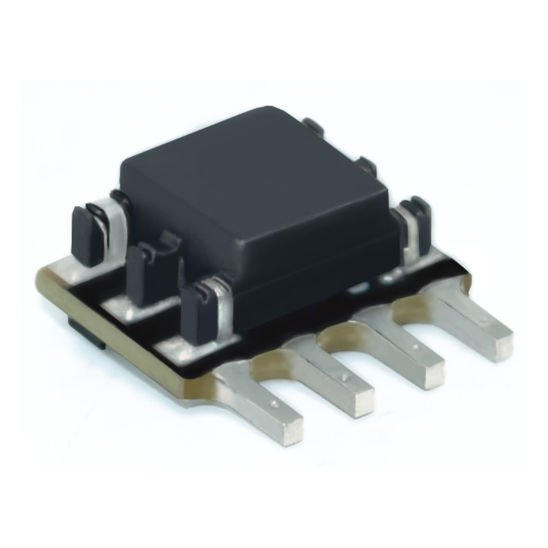
The ADMV8818 is a highly flexible filter in a 9mm × 9mm package that provides tunable bandpass, highpass, lowpass or bypass response between 2GHz and 18GHz. The chip consists of two parts: input part and output part. The input section has four high-pass filters and an optional bypass, which is selectable via two RFIN switches. Likewise, the output section has four low-pass filters and an optional bypass, which is selectable via two RFOUT switches. Each high-pass and low-pass filter can be tuned with 16 states (4 control bits) to adjust the 3dB frequency (f3 dB). Figure 10 shows the functional block diagram of the ADMV8818.

Figure 10. ADMV8818 functional block diagram
With a flexible structure that can be quickly reconfigured and a small form factor, the ADMV8818 provides full coverage in the 2GHz to 18GHz frequency band without any dead zones. The ADMV8818 can be configured as a suboctave preselect filter, mirror, or IF filter. When configured in the signal chain shown in Figure 11, the receiver can maintain high sensitivity and can operate in the presence of large OWhen using OB signal, ADMV8818 is used as the preselector instead.

Figure 11. Block diagram of a 2 Ghz to 18 GHz receiver using the ADMV8818 as preselector and image filter.
For example, if a target signal is received near the 9GHz band, but there is a strong OOB blocker signal in the 4.5GHz band, then the blocker signal will cause harmonics to appear near the 9GHz target signal, hampering operation. Configuring the ADMV8818 as a 6GHz to 9GHz bandpass filter allows broadband signals to pass while appropriately reducing the level of blocking signals before causing harmonic problems in the nonlinear elements of the signal chain. The S-parameter sweep of the ADMV8818 configured for this situation covers the blocking signal, as shown in Figure 12.

Figure 12. ADMV8818 configured as a 6GHz to 9GHz bandpass filter. This filter suppresses F2–F1, F1+F2, F/2, and F×2 spurious products.
A size comparison of typical 2GHz to 18GHz preselected filter modules is shown in Figure 13. Among them, the switch-fixed filter preselector group is implemented on a ceramic substrate using distributed filtering technology. The size is estimated based on filter products on the market. An eight-throw switch is included in the estimate to compare equivalent functionality. The tunable BPF shown in the figure is the ADMV8818, which covers the same frequency range and has more comprehensive tuning flexibility than the switched filter bank. Compared with a switched filter bank, the ADMV8818 saves more than 75% of its area. The preselector function in the receiver signal chain often accounts for a significant proportion of the overall system size, so this area saving is critical in size-constrained systems that can flexibly trade between size and performance. make trade-offs.

Figure 13. Fixed-switched 2 GHz to 18 GHz BPF (left) versus digitally tunable 2 GHz to 18 GHz BPF (right). The occupied area is saved by more than 75%.
The ADMV8913 is a combination high-pass and low-pass filter in a 6mm × 3mm package. It is specifically designed to operate in the frequency range from 8Ghz to 12GHz (X-band) with an insertion loss as low as 5dB. Both high-pass and low-pass filters can be tuned with 16 states (4 control bits) to adjust the 3dB frequency (f3 dB). In addition, the ADMV8913 integrates a parallel logic interface that can set the filter state without requiring SPI communication. This parallel logic interface is useful for systems requiring fast filter response times because it eliminates the time required for SPI processing. Figure 14 shows the functional block diagram of the ADMV8913.

Figure 14. ADMV8913 functional block diagram
Modern X-band radar systems, whether using mechanically steered antennas or high-channel-count phased array beams, typically rely on filtering solutions that are compact, have low insertion loss, and are easy to configure. The ADMV8913 is ideally suited for this application due to its low insertion loss, small size, and flexible digital interface options (SPI or parallel control). These features enable it to be placed close to the front-end of these systems, ensuring excellent performance while reducing integration complexity.
In conclusion
There are many factors to consider when designing the RF front-end for a wideband receiver. The front-end must be designed to handle unpredictable blocking conditions while still detecting low-level signals. The ability to dynamically adjust the front-end filtering performance to handle these blocking signals is a key feature of the RF front-end. ADI's new digitally controlled tunable filter IC products have excellent performance and enhanced digital functions to meet the needs of many front-end applications. These two new products are just the first of many new developments in the Digital Tunable Filters portfolio. Customers interested in learning about these products should visit the Digital Tunable Filters product page to view the latest datasheet, or contact a local representative to discuss specific end applications.
Digital tunable filters (DTFs) have revolutionized the field of signal processing and have become an essential component in wideband receiver applications. These filters offer the flexibility and adaptability required to support the demanding requirements of modern wideband receivers.
A digital tunable filter is a type of filter that can be adjusted or tuned to different frequency ranges digitally. Unlike traditional fixed filters, DTFs provide the ability to dynamically change the filter characteristics, such as center frequency, bandwidth, and filter shape. This allows for precise control and optimization of the filter response to match the specific requirements of the wideband receiver.
One of the key advantages of DTFs in wideband receiver applications is their ability to handle a wide range of frequencies. Wideband receivers are designed to receive signals across a broad frequency spectrum, often spanning multiple bands. With a DTF, the filter can be digitally adjusted to select the desired frequency range, enabling the receiver to effectively capture and process signals within that range.
Furthermore, DTFs offer excellent selectivity and rejection capabilities. Wideband receivers often operate in environments with high levels of interference and noise. The ability of DTFs to selectively filter out unwanted signals and reject noise ensures that only the desired signals are processed, improving the overall signal quality and reducing the impact of interference.
Another advantage of DTFs is their flexibility in adapting to changing signal conditions. Wideband receivers may encounter varying signal strengths and dynamic range requirements. DTFs can be dynamically adjusted to adapt to these changing conditions, allowing the receiver to maintain optimal performance across different signal scenarios.
Moreover, DTFs offer programmability and configurability, making them highly versatile in wideband receiver applications. The filter parameters can be easily adjusted through digital control, allowing for real-time adaptation and optimization. This flexibility enables the receiver to accommodate different signal types, modulation schemes, and bandwidth requirements.
In conclusion, digital tunable filters play a vital role in supporting wideband receiver applications. Their ability to dynamically adjust the filter characteristics, handle a wide range of frequencies, provide excellent selectivity and rejection, adapt to changing signal conditions, and offer programmability make them an essential component in modern wideband receivers. The flexibility and adaptability of DTFs enable receivers to effectively process signals across a broad frequency spectrum, improving overall performance and signal quality in diverse and challenging environments.

