


CTSD ADC—Part 1 How to Improve Precision ADC Signal Chain Design
Summary
Precision signal chain designers are faced with the challenge of meeting noise performance requirements in medium-bandwidth applications, often ending up with a trade-off between noise performance and accuracy. Reducing time to market and getting the design right the first time adds further pressure. The inherent architectural advantages of the duration Σ-Δ (CTSD) ADC simplify the signal chain design, thereby reducing the solution size and helping customers shorten the time to market of end products. To illustrate the architectural advantages of the CTSD ADC itself and how it can be used in a variety of precision medium-bandwidth applications, we will provide an in-depth analysis of the signal chain design to allow designers to understand the key advantages of CTSD technology and explore the ease of design features of the AD4134 precision ADC.
Introduction
In many digital processing applications and algorithms, over the past 20 years there has been an increasing requirement for higher resolution and accuracy in all converter technologies. By using an external digital controller, software techniques such as averaging and optimized filtering schemes can extract and provide more accurate results, improving the ADC's limited resolution/accuracy. To reduce the extensive post-processing work of a digital microcontroller or DSP, designers can use high-performance precision ADCs. This will reduce optimization time on the digital side and may also consider using a lower cost microcontroller or DSP. The applications and markets for precision ADCs are wide:
►Industrial instrumentation: vibration analysis, temperature/pressure/stress/flow measurement, dynamic signal analysis, acoustic analysis

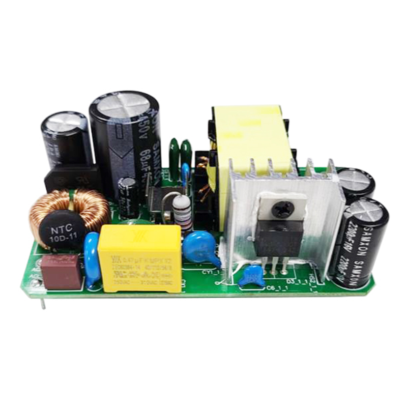
Figure 1. Precision ADC signal chain example
►Medical instrumentation: electrophysiology, blood analysis, electrocardiogram (EKG/ECG)
►Defense applications: sonar, telemetry
►Test and measurement: audio testing, hardware looping, power quality analysis
The analog input signals processed by the ADC can be sensor signals with voltage and current outputs, or feedback control loop signals with bandwidths ranging from DC to hundreds of kHz. The ADC digital output format and rate depend on the application and post-processing required by the following digital controller. Generally speaking, signal chain designers follow the Nyquist sampling rule and set the ADC output data rate (ODR) of the digital controller to at least twice the input frequency. Most ADCs allow flexible adjustment of the output data rate based on the relevant signal band.
With currently available ADCs, several signal conditioning stages are involved before the ADC can interact with the input signal. Signal conditioning circuits with stringent requirements need to be designed and customized around the specific and individual ADC technology to ensure that the performance of the ADC datasheet is achieved. The signal chain designer's job does not end after selecting an ADC. It often takes a lot of time and effort to design and tune peripherals. Analog Devices' design simulation tools and model libraries provide designers with technical support to help them meet design challenges.
New Approach: Simplifying the Design Journey with CTSD Architecture
Primarily used in audio and high-speed ADCs, the CTSD architecture is now tailored for precision applications, enabling high accuracy while leveraging its unique signal chain simplicity. Leveraging this architecture reduces the workload of designing peripherals. Figure 2 shows just a small part of how the current ADC signal chain can be simplified and reduced by 56% by using this new solution to achieve high channel density.
To illustrate how CTSD ADC technology can simplify signal chain design, this article highlights some of the key challenges involved in existing signal chains for general applications and demonstrates how CTSD ADCs mitigate these challenges.
Therefore, we first introduce several design steps involved in an existing signal chain. The first task is to select the right ADC for the target application.
Step 1: Select ADC
In addition to the resolution and accuracy of the final digital output required by the application, the signal bandwidth, ODR, signal type and range to be processed are also important considerations when selecting an appropriate ADC from the wide range available. Generally speaking, in most applications, digital controllers require the use of algorithms to process the amplitude, phase, or frequency of the input signal.
In order to accurately measure any of the previous factors, the error added during the digitization process needs to be minimized. The major errors and their corresponding measurement terms are detailed in Table 1, and further details are provided in the Basic Guide to Data Conversion.
The performance indicators in Table 1 are related to signal amplitude and frequency and are often referred to as AC performance parameters.
For DC or near-DC applications, such as power metering that handles 50 Hz to 60 Hz input signals, ADC errors such as offset, gain, INL, and flicker noise must be considered. These DC performance parameters also require some temperature stability for the intended use of the application.
Analog Devices offers a variety of industry-leading, high-performance ADCs to meet the system needs of multiple applications, such as those based on accuracy, speed, or limited power budgets. Merely comparing two sets of ADC specifications is not enough to make the correct ADC selection. Overall system performance and design challenges must also be considered, which is key when choosing an ADC technology or architecture. Two broad categories of ADC architectures are traditionally preferred. Commonly used are Successive Approximation Register (SAR) ADCs, which follow the simple Nyquist criterion. It states that a signal can be reconstructed if sampled at twice its frequency. The advantages of SAR ADCs are excellent DC performance, small size, low latency, and power regulation through ODR.
The second technology option is a discrete-time Σ-Δ (DTSD) ADC, which works on the principle that the larger the number of samples, the less information is lost. Therefore, the sampling frequency is much higher than the specified Nyquist frequency, a scheme called oversampling. This architecture also has the advantage that the error added due to sampling is minimized within the frequency band of interest. Therefore, the DTSD ADC combines excellent DC and AC performance, but with higher latency.

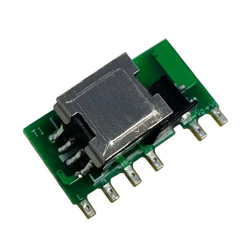
Figure 2. Small form factor solution with ADI’s easy-to-use new CTSD ADC
Figure 3 shows typical analog input bandwidths for SAR and DTSD ADCs, along with some common product options for different speeds and resolutions. You can also use the sophisticated quick search function to help you select an ADC.
Additionally, a new type of precision ADC is now available. These ADCs are based on DTSD ADCs and have comparable performance to DTSD ADCs, but have unique advantages in simplifying the entire signal chain design process. This new ADC family addresses some of the more prominent challenges in subsequent design steps of existing signal chains.
Step 2: Input and ADC Interface
A sensor whose output is processed by an ADC may have very high sensitivity. Designers must have a clear understanding of the ADC input structure that the sensor will interface with to ensure that ADC errors do not affect or distort the actual sensor signal.
In traditional SAR and DTSD ADC, the input structure is called a switched capacitor sample and hold circuit, as shown in Figure 4. On each sample clock edge, when the sample switch changes its ON/OFF state, it needs to support a limited current requirement to charge and discharge the hold capacitor to a new sample input value. This current needs to be supplied by an input source, which in the example we are discussing is a sensor. In addition, the switch itself has some on-chip parasitic capacitance, which will inject some charge into the power supply, called charge injection kickback. The resulting increased error source also needs to be absorbed by the sensor to avoid adversely affecting the sensor signal.
Most sensors are unable to provide this current amplitude, indicating that they cannot drive switching circuits directly. In the other case, even if the sensor is capable of supporting these current demands, the sensor's finite impedance will add error at the ADC input. The charge injection current is a function of the input and this current will cause an input-related voltage drop across the sensor impedance. As shown in Figure 4a, the input to the ADC is wrong. Placing a driver amplifier between the sensor and the ADC can solve these problems, as shown in Figure 4b.
Now we need to set the standard for this amplifier. First, the amplifier should support charging current and be able to absorb charge injection kickback. Second, the amplifier's output needs to be completely stable at the end of the sampling edge so that no error is added when sampling the ADC input. This means that the amplifier should be able to deliver transient current steps, mapped to having a high slew rate, and provide a fast settling response to these transient events, mapped to having a high bandwidth. As the sampling frequency and resolution of ADCs increase, meeting these requirements becomes critical.
One of the challenges faced by designers, especially those dealing with medium-bandwidth applications, is determining the appropriate amplifier for the ADC. As mentioned before, ADI provides a set of simulation models and precision ADC driver tools to simplify this step, but for the designer, this is an additional design step to achieve the ADC data sheet performance. Some new-age SAR and DTSD ADCs address this challenge by using novel sampling techniques to completely reduce transient current requirements, or by employing integrated amplifiers. But both solutions limit the range of signal bandwidth or impair the performance of the ADC.
Advantages of CTSD ADC: CTSD ADC solves this problem by providing new options for easy-to-drive resistive inputs instead of switched capacitive inputs. This shows that there is no hard requirement for a high bandwidth, high slew rate amplifier. If the sensor can directly drive this resistive load, it can interface directly with the CTSD ADC; otherwise, any low-bandwidth, low-noise amplifier can be connected between the sensor and the CTSD ADC.

Figure 3. Precision ADC architecture positioning

Figure 4. (a) Switched capacitor charge injection kickback to sensor, (b) use of input buffer to isolate kickback effect
Step 3: Reference voltage source and ADC interface
Interfacing with a voltage reference involves similar challenges as interfacing with an input. The reference voltage source input of a traditional ADC is also a switched capacitor. On each sample clock edge, the reference needs to charge the internal capacitor, thus requiring a large switching current with good settling time.
Available reference ICs do not support large switching current requirements and have limited bandwidth. The second interface challenge is that the noise from these voltage references is greater than the noise of the ADC. To filter out this noise, a first order RC circuit is used. On the one hand, we limit the bandwidth of the reference to reduce noise, and on the other hand, we need fast settling time. These are two opposing requirements that need to be met simultaneously. Therefore, a low-noise buffer is used to drive the ADC reference pin, as shown in Figure 5b. The slew rate and bandwidth of this buffer are determined based on the sampling frequency and resolution of the ADC.
Likewise, like our precision input driver tools, ADI also provides tools for ADC simulation and selecting the correct reference buffer. As with the inputs, some new-age SAR and DTSD ADCs also offer an integrated reference buffer option, but with performance and bandwidth limitations.
Advantages of CTSD ADCs: Using a CTSD ADC allows you to skip this design step entirely, as it provides a new and easy option for driving resistive loads without the need for such high-bandwidth, high-slew-rate buffers. Reference ICs with low-pass filters interface directly to the reference pins.
Step 4: Make the signal chain immune to interference
Sampling and digitizing a continuous signal results in a loss of information, which is called quantization noise. The sampling frequency and number of bits determine the performance limits of the ADC architecture. After addressing the performance and interface challenges of the reference and inputs, the next challenge is to address the folding of high-frequency (HF) interference sources/noise into the target low-frequency bandwidth. This is called aliasing or folding. The reflected image of these high-frequency or out-of-band interferers entering the bandwidth of interest results in reduced signal-to-noise ratio (SNR). Due to sampling guidelines, any tones around the sampling frequency will fold back in-band, as shown in Figure 6, producing unnecessary information or errors within the target frequency band. For more details on aliasing, see Tutorial MT-002: What the Nyquist Criterion Means for Data Sampling System Design.

Figure 5. (a) Switched capacitor charge injection kickback to reference IC (b) Use of reference buffer to isolate kickback effects

Figure 6. Out-of-band interferers aliased/folded into the target band due to sampling

Figure 7. Using anti-aliasing filters to mitigate aliasing effects on in-band performance
One solution to mitigate the foldback effect is to use a low-pass filter called an anti-aliasing filter (AAF) to attenuate the amplitude of the unwanted interferer so that when the attenuated interferer folds back into the band, the desired signal-to-noise ratio. This low-pass filter is usually integrated with a driver amplifier, as shown in Figure 7.
The biggest challenge when designing this amplifier was finding a balance between fast settling and low-pass filtering requirements. Another challenge is that the solution needs to be fine-tuned for each application's needs, which limits the use of a single platform design for each application. ADI has many anti-aliasing filter tool designs to help designers overcome this challenge.
Advantages of CTSD ADC: This interference immunity can be solved by the aliasing suppression characteristic of CTSD ADC itself, which is a unique characteristic of CTSD ADC. ADCs using this technology do not require AAF. Therefore, we are one step closer to easily connecting the CTSD ADC directly to the sensor.
Step 5: Select ADC clock frequency and output data rate
Next, let's discuss the clocking requirements of the two traditional ADC types. DTSD is an oversampled ADC, which is an ADC that samples at a higher than Nyquist sampling rate. However, providing the ADC oversampled data directly to an external digital controller will overload it with a large amount of redundant information. In an oversampling system, the core ADC output is decimated using on-chip digital filters, resulting in a lower data rate for the final ADC digital output, typically twice the signal frequency.
For DTSD ADCs, designers need to plan to provide a high-frequency sampling clock to the core ADC and set the required output data rate. The ADC will provide the final digital output at this required ODR and ODR clock. The digital controller uses this ODR clock to input data.
Next, we address the clocking requirements of the SAR ADC, generally following the Nyquist criterion. Here, the sampling clock of the ADC is provided by the digital controller, and the clock also acts as the ODR. However, since the sample-and-hold timing needs to be effectively controlled to obtain excellent performance from the ADC, this clock has less timing flexibility, which also means that the digital output timing needs to be as consistent as possible with these requirements.

Figure 8. Clock requirements for (a) DTSD ADC and (b) SAR ADC
Understanding the clocking requirements for both architectures, you can see that the ODR is coupled to the ADC's sampling clock, which is a limiting factor in many systems where the ODR can drift or change dynamically or needs to be tuned to the frequency of the analog input signal.
Advantages of CTSD ADC: The CTSD ADC can be coupled with a new asynchronous sample rate converter (ASRC), which can resample the core ADC at any desired ODR. ASRC also enables designers to precisely set ODR to any frequency, breaking the old limitation of limiting ODR to multiples of the sampling frequency. ODR The frequency and timing requirements are now fully within the capabilities of the digital interface and are independent of the ADC sampling frequency. This feature simplifies digital isolation design for signal chain designers.
Step 6: Interface with external digital controller
Traditionally, there are two types of data interface modes for ADC communication with digital controllers. One type uses the ADC as a master, providing the digital/ODR clock and determining the clock edges of the digital controller for input ADC data. The other type is managed mode (receiver mode), where the digital controller is the host, provides the ODR clock, and determines the clock edges of the input ADC data.
Starting with step 5, if the designer selects a DTSD ADC, this ADC will provide the ODR clock and therefore act as a host for the following digital controller. If the SAR ADC is selected, the digital controller needs to provide the ODR clock, which means the SAR ADC will always be configured as a managed peripheral. Therefore, there are obvious limitations: once the ADC architecture is chosen, the digital interface is limited to host mode or managed mode. Currently, regardless of the ADC architecture, there is no flexibility in interface selection.
CTSD ADC Advantages: The new ASRC combined with the CTSD ADC enables designers to independently configure the ADC data interface mode. This opens up entirely new opportunities for applications where high-performance ADCs can be configured in any mode suitable for digital controller applications, regardless of ADC architecture.
Connect the devices
Figure 9 shows the building blocks of a traditional signal chain, with an analog front end (AFE) consisting of an ADC input driver, an alias rejection filter, and a reference buffer that can be greatly simplified by a CTSD ADC. Figure 10a shows an example signal chain using a DTSD ADC that requires significant design effort to fine-tune and determine the ADC’s datasheet performance. To simplify the process for customers, ADI provides reference designs that can be reused or repurposed for various applications with these ADCs.
Figure 10b shows the signal chain with a CTSD ADC and its simplified analog input front end (AFE) because its ADC core does not have switched capacitor samplers on the input and reference voltage source sides. The switching sampler is moved to the last stage of the ADC core, making the signal input and reference input purely resistive. The result is an ADC with virtually no sample aliasing, putting it in a class of its own. In addition, the signal transfer function of this type of ADC simulates an anti-aliasing filter response, which means that it inherently attenuates noise interference sources. Using CTSD technology, the ADC can be reduced to a simple plug-and-play component.
In summary, the CTSD ADC simplifies signal chain design while enabling a system solution with the same performance level as a traditional ADC signal chain, with the following advantages:
►Provides an alias-free, low-latency signal chain with excellent channel-to-channel phase matching
►Simplified analog front-end, eliminating the additional steps of selecting and fine-tuning high-bandwidth input and reference drive buffers, enabling higher channel density
►Breaks the barrier that ODR is a function of the sampling clock
►Independent control interface with external digital controller
►Improved signal chain reliability ratings, a benefit of fewer peripheral components
►Reduced size, BOM reduced by 56%, shortening product time to market for customers
The next article in this series will explore how CTSD ADCs and ASRCs can help simplify signal chain design. The next few articles in this series will introduce the concepts of CTSD ADC and ASRC in more detail, focus on the advantages of the signal chain, and finally explain how to take advantage of the features of the new product AD4134. Stay tuned to learn more about breakthrough CTSD and ASRC technologies that help simplify design!

Figure 9. Signal chain building blocks using traditional precision ADC and CTSD ADC respectively.

Figure 10. Example signal chain using (a) DTSD technology and (b) CTSD technology
Acknowledgments
The authors would like to thank Naiqian Ren and Mark Murphy for their helpful insights in writing this article.
References
“Application Note AN-282: Fundamentals of Sampled Data Systems.” Analog Devices
Driving Precision Converters: Selecting a Reference Source and Amplifier. Analog Devices
Kester, Walt. “MT-021 Tutorial: ADC Architecture II: Successive Approximation ADC.” Analog Devices, Inc., 2009.
Σ-Δ ADC Guide. Analog Devices
Shaikh, Wasim and Srikanth Nittala. “Build AC and DC data acquisition signal chains with ease.” Analog Dialogue, Volume 54, Issue 3, August 2020.
Trail:
CTSD Precision ADC — Part 2: Introducing the CTSD Architecture for Signal Chain Designers
This article will introduce continuous-time sigma-delta (CTSD) ADC technology in a different way than the traditional approach, so that signal chain designers can understand this new and easy-to-use precision ADC technology and think of it as a connection between some of the existing A simple system that knows its components. In Part 1, we highlighted key challenges in existing signal chain designs that can be significantly simplified by utilizing precision CTSD ADCs to achieve high accuracy while maintaining continuous-time signal integrity. The question now is what is behind the CTSD architecture that enables it to achieve these advantages?
Step 1: Review Closed Loop Inverting Amplifier Configuration
Step 2: Introducing Discrete Components into the Amplifier
Step 3: Introducing the Analog Accumulator – Integrator
Step 5: Understand Oversampling
Step 6: Understand Noise Shaping
Step 7: Complete the CTSD Modulator with Digital Filters
Step 8: Understand the Clock Sensitivity of the CTSD ADC
Step 9: Voila! Everything is ready to explain the concept of CTSD to your friends!