


Super Detailed Phase-shifting Full Bridge Study Notes
Due to my work relationship, I have recently come into contact with phase-shifted full-bridge power supplies. Since I have never been exposed to this aspect of power supply before, I am completely blank about the principles and practical experience. The purpose of this post is to share my learning process and experience with everyone. Sharing, during this process, there may be some misunderstandings or extreme views. Please feel free to point them out and help me correct them. In short, this will be a process of improvement together with everyone.
I have searched on the Internet and there are very few articles explaining the working principle of the phase-shifted full bridge. This is another reason why I opened this post. One thing that needs to be explained is that I drew all the drawings by myself using PROTEL99. There may be some differences with professional software, so just make do with it!
In early high-power power supply (output power greater than 1KW) applications, the hard-switched full-bridge topology was the most widely used. It is characterized by a fixed switching frequency and small voltage and current stress on the switching tube. Easy to control, especially suitable for situations with low voltage, large current, and large changes in output voltage and current. However, due to the loss of switching devices, the switching frequency cannot be increased to obtain higher power density. For example: a 5KW power supply uses a hard-switched full bridge. Even if the efficiency reaches 92%, there will still be a loss of 400W. Each time the efficiency is improved by one point, the loss can be reduced by 50W, especially when multiple machines are paralleled and In systems that run for a long time, the economic benefits are considerable.
Subsequently, based on the hard-switching full-bridge, people developed a soft-switching full-bridge topology—Phase-Shifting Full-Bridge Converter (PS FB), which uses the junction capacitance of the power device and The leakage inductance of the transformer acts as a resonant component, causing the four switching tubes of the full-bridge power supply to conduct in sequence at zero voltage (Zero voltage Switching, ZVS) to achieve constant frequency soft switching and improve the overall efficiency and EMI performance of the power supply. Of course, It can also increase the power density of the power supply.

The above picture is the topology diagram of the phase-shifted full bridge. The meaning of each component is as follows:
Vin: Input DC power
T1-T4: 4 main switch tubes, usually MOSFET or IGBT
T1 and T2 are called super forearm switching tubes, and T3 and T4 are called lagging arm switching tubes.
C1-C4: Parasitic capacitance of 4 switching tubes or external resonant capacitance
D1-D4: Parasitic diodes of 4 switching tubes or additional freewheeling diodes
VD1, VD2: power supply secondary high frequency rectifier diode
TR: Phase-shifted full-bridge power transformer
Lp: Transformer primary winding inductance
Ls1, Ls2: transformer secondary inductance
Lr: The primary leakage inductance of the transformer or the sum of the primary leakage inductance and the external inductance
Lf: Phase-shifted full-bridge power supply secondary output freewheeling inductor
Cf: phase-shifted full-bridge power supply secondary output capacitor
RL: Phase-shifted full-bridge power supply secondary load
Because this is a theoretical analysis, it is necessary to idealize the characteristics of some devices, as follows:
Assume that all switching tubes are ideal components, there is no delay between turning on and off, and the on-resistance is infinitesimal; the body diode or external diode of the switching tube is also an ideal component, there is no delay between turning on and off, and the forward voltage drop is 0.
All inductors and capacitors are ideal components, and there are no parasitic parameters. The transformer is also an ideal transformer, and there is no influence of leakage inductance and distribution parameters. The excitation inductance is infinite, the excitation current can be ignored, and the resonant inductance is external.
The leading bridge arm and lagging resonant capacitance are equal, that is, C1=C2=Clead, C3=C4=Clag.
The inductance LS` converted from the secondary freewheeling inductor to the primary through the turns ratio is much larger than the inductance Lr of the resonant inductor, that is, LS`=Lr*n2》Lr.
One cycle of PS FB can be divided into 12 working modes. The positive and negative half cycles are corresponding relationships, but what changes is the flow direction of the current on the bridge arm. Let's first analyze the situation of these 12 working modes. Uncover the mystery of the phase-shifted full bridge.

Working mode 1: Positive half-cycle power output process
As shown in the figure above, at this time, T1 and T4 are turned on at the same time, T2 and T3 are turned off at the same time, and the flow direction of the primary current is T1-Lp-Lk-T4, as shown in the figure.
At this time, the input voltage almost all falls on the two points A and B in the figure, that is, UAB = Vin. At this time, in addition to the Lp and Lk marked on the figure, the inductance at the two points AB should also have secondary reflections. The returned inductance LS` (because the secondary diode VD1 is conductive at this time), that is, LS`=n2* Lf, is converted back according to the square of the turns ratio, so LS` will be much larger than Lk, causing Ip to rise slowly. The rising current △Ip is
△Ip=(Vin-n*Uo)*(t1-t0)/( Lk+ LS`)
During this process, according to the relationship between the terminals of the same name of the transformer, the secondary diode VD1 is turned on and VD2 is turned off. The primary side of the transformer provides energy to the load and stores energy to the output inductor Lf and output capacitor Cf. (not shown in the picture)
At this time, UC2 =UC3=UA=UAB=Vin
UB=0V

Working mode two: super forearm resonance process
As shown in the figure above, the leading bridge arm upper transistor T1 is turned off at time t1. However, due to the characteristic that the current at both ends of the inductor cannot change suddenly, the current on the primary side of the transformer still needs to maintain its original direction, so the current is transferred to C1 and C2. C1 is charged, and the voltage will soon rise to the input voltage Vin, while C2 begins to discharge, and the voltage will soon drop to 0, which means the potential at point A is clamped to 0V.
Since the converted inductance LS` of the secondary is much larger than the inductance Lk of the resonant inductor, it can be basically considered that the primary side is similar to a constant current source, and the ip at this time is basically unchanged or decreases very little.
The voltage across C1 is given by
Vc1=Ip*(t2-t1)/(C1+C3)= Ip*(t2-t1)/2 Clead
The voltage across C2 is given by
Vc1= Vin-【Ip*(t2-t1)/2 Clead】
Among them, Ip is the current flowing through the primary inductor in mode 2. At time T2, the voltage on C1 quickly rises to Vin, the voltage on C2 quickly becomes 0V, and D2 begins to conduct.
Before time t2, C1 is fully charged and C2 is fully discharged, that is, VC1= VC3= Vin VC2=VA=VB= 0V
The time of mode 2 is:
△t= t2-t1=2 Clead * Vin/ Ip

Working mode three: primary side current positive half-cycle clamping freewheeling process
As shown in the figure above, at this time, diode D2 has completely conducted freewheeling, clamping the voltage at both ends of the super forearm lower tube T2 to 0V. At this time, opening T2 will realize the ZVS turn-on of the super forearm lower tube T2; but at this time The primary current still flows from D2, not T2.
At this time, the current flowing through the primary side is still large, and the current of the secondary inductor Lf is converted into the current of the primary side.
That is ip(t)= iLf(t)/n
At this time, the rate of decline of the current is related to the inductance.
The period of time td from the turning off of the super forearm T1 to the turning on of T2 is called the super forearm dead time. In order to ensure that the ZVS opening condition of T2 is met, C3 must be discharged to 0V, that is
td ≥△t= t2-t1=2 Clead * Vin/ Ip
At this time, UC1=UC3=Vin, UA=UB=UAB=0V

Working mode four: Positive half-cycle lag arm resonance process
As shown in the figure: at time T3, the lagging arm lower tube T4 is turned off. Before T4 is turned off, the voltage across C4 is 0, so T4 is turned off at zero voltage. Due to the turn-off of T4, the primary current ip suddenly loses its path. However, according to the principle of inductance, we know that the primary current is not allowed to mutate and needs to maintain its original direction and decrease at a certain rate. Therefore, the primary current ip will charge C4, causing the voltage across C4 to slowly rise, and at the same time draining away the charge across C3.
That is ip(t)=I2sinω(t-t3)
vc4(t)=ZpI2sinω(t-t3)
vc3(t)=Vin-ZpI2sinω(t-t3)
Among them, I2: at time t3, the current value after the primary current decreases
Zp: Resonant impedance of the lagging arm, Zp= )0.5
ω: Resonant angular frequency of the lagging arm, ω=1/(2Lr*Clag)0.5
Some people may wonder why the current has a sinusoidal function relationship. Yes, because at this time, the resonant inductor Lr on the primary side resonates with the two capacitors C3 and C4 of the lagging arm, and the relationship is a sinusoidal relationship. Why did I mention above that only the primary resonant inductor Lr participates in resonance, then does the secondary energy storage inductor participate in resonance? Let’s analyze it below:
Since the lower tube T4 of the lagging arm is turned off, C4 slowly builds up a voltage, which is finally equal to the power supply voltage, that is, UC4=Vin. From the drawing, we can see that UC4 is actually the voltage at point B, and the voltage across C4 rises. It is the process of the voltage at point B slowly rising from 0V, and at this time the voltage at point A is clamped to 0V, so this will cause UAB<0V, which means that the voltage of the primary winding has begun to reverse at this time.
Due to the reverse direction of the primary voltage, LS1 and LS2 have a positive and upward relationship at the same time according to the relationship between the terminals of the same name. At this time, VD2 begins to conduct and current flows; and due to the relationship between LS1 and Lf, the current flowing through LS1 and VD1 The current cannot be reduced to 0 immediately, but can only be reduced slowly; and the current through VD2 can only be slowly increased, so VD1 and VD2 are turned on at the same time, that is, the secondary windings LS1 and LS2 are short-circuited at the same time. .
The short circuit of the secondary winding causes the path of Lf to be reflected to the primary side to be cut off, which means that the inductance of the primary side participating in the resonance is rapidly reduced from the original (Lf*n2+ Lr) to only Lr. Since the Lr ratio (Lf*n2+ Lr) is much smaller, so the primary current will decrease rapidly.
At this time, UAB=ULr=-Vin on the primary side, UA=0V, UB= Vin

Switching mode five: resonance ends, the primary inductor feeds energy to the grid
As shown in the figure, when C4 is charged to Vin, the resonance ends, and no current flows through C3 and C4. Instead, D3 naturally conducts, and the primary current feeds energy to the grid through D2-Lr-D3. In fact, the energy source Due to the energy stored in Lr, the primary current decreases rapidly at this time, ip(t) = Ip4- (t-t4) where Ip4 is the primary current value at t4 and decreases to 0 at t5. At this time, the voltage at both ends of T3 drops to 0V. As long as T3 is turned on at this time, T3 will achieve the effect of zero voltage turn-on.
There are several concepts that need to be introduced here:
Dead time: The upper and lower tubes of the super forearm or lagging arm, the interval time between turning on or off, the phase-shifted full-bridge power supply has 4 dead time in each cycle.
Resonance period: After the two tubes of the lagging arm are turned off and before the two tubes of the super forearm are turned on, the sum of the inductance and the resonant inductance reflected by the secondary inductor through the turns ratio and the respective resonant capacitances are two resonance times; there is also the super The forearm has been turned on, and before the two tubes of the lagging arm commutate, the resonant inductor and their respective resonant capacitors have two resonance times.
Phase shift angle: refers to the time interval from the opening of the super forearm upper tube to the opening of the lagging arm lower tube or the time interval from the super forearm lower tube opening to the opening of the lagging arm upper tube, and then converted into an angular frequency ω
ω=2∏f=2∏/T.
For switching mode 5, the resonance period must be smaller than the dead time, otherwise the ZVS effect of the lagging arm cannot be achieved. However, the resonant inductor at this time does not have the secondary inductance reflected back through the turns ratio, so only the resonant inductor participates in the resonance. Be careful when designing. The resonant inductor must be large enough. Otherwise, if the resonant energy is not enough, the primary current will will be distorted.
At time t5, UAB=ULr=-Vin, UA=0V, UB= UC1= Vin

Switching mode six: The primary current increases in the reverse direction from 0
As shown in the figure, before time t5, T3 has been turned on. At time t5, the primary current ip has dropped to 0. Since there is no current, D2 and D3 are naturally turned off.
During the period of t5-t6, the diodes D1 and D2 on the secondary side are still conducting and flowing current at the same time, short-circuiting the secondary winding and blocking the reflection path of the output inductor to the primary. At this time, the load current is still caused by the secondary inductor and The output capacitor provides; at the same time, because the primary side T2 and T3 have been turned on, the primary side current ip flows through T3--Lr--T2, and because Lr is very small, the primary side current ip will increase sharply in the opposite direction.
That is ip(t)= - (t-t5)
At time t6, ip reaches the maximum, which is equal to the secondary inductor current converted to the primary current.
That is ip(t6)= - ILf(t6)/n
In this switching mode, the primary current does not transfer energy, but there is a violent commutation process on the secondary side. The current through the secondary diode VD1 decreases rapidly, and the current through VD2 increases rapidly. At time t6, through The current of VD1 decreases to 0, and the current through VD2 is equal to the inductor current ILf.
After reaching time t6, the positive half-cycle work of the phase-shifted full bridge ends; and the negative half-cycle work begins. Its working principle is similar to the positive half-cycle. Further analysis is done below: before time t6, the UAB of the primary side = ULr =-Vin,UA=0V, UB=Vin

Switching mode seven: negative half-cycle power output process
As shown in the figure above, at this time, T2 and T3 are turned on at the same time, T1 and T4 are turned off at the same time, and the flow direction of the primary current ip is T3-Lk-Lp-T2, as shown in the figure.
At this time, the input voltage almost all falls on the two points B and A in the figure, that is, UAB = -Vin. At this time, in addition to the Lp and Lk marked on the figure, the inductance of the two points AB should also have a secondary The reflected inductance LS` (because the secondary diode VD2 is conductive at this time), that is, LS`=n2* Lf. Since it is converted back according to the square of the turns ratio, LS` will be much larger than Lk, causing Ip to rise slowly. , the rising current △Ip is
-△Ip=-【 (Vin-n*Uo)*(t7-t6)/( Lk+ LS`)】
During this process, according to the relationship between the terminals of the same name of the transformer, the secondary diode VD2 is turned on and VD1 is turned off. The primary side of the transformer provides energy to the load and stores energy to the output inductor Lf and output capacitor Cf. (not shown in the picture)
At this time, UC1 =UC4=UB =Vin UAB=-Vin
UA=0V

Switching mode eight: Negative half-cycle super forearm resonance process
As shown in the figure above, at this time, the leading bridge arm lower tube T2 is turned off at t7. However, due to the characteristics of the current at both ends of the inductor that cannot change suddenly, the current on the primary side of the transformer still needs to maintain its original direction, so the current is transferred to C1 and C2. C2 is charged, and the voltage will soon rise to the input voltage Vin, and the charge of C1 will be quickly removed, and the voltage across C1 will soon drop to 0V, which means the potential of point A is clamped to Vin.
Since the converted inductance LS` of the secondary is much larger than the inductance Lk of the resonant inductor, it can basically be considered that this Yes, the primary side is similar to a constant current source. At this time, the IP is basically unchanged, or the decrease is very small.
The voltage across C2 is given by
Vc2=︱-Ip︱*(t8-t7)/(C1+C2)= Ip*(t8-t7)/2 Clead
The voltage across C1 is given by
Vc1= Vin-【︱-Ip︱*(t8-t7)/2 Clead】
Among them, Ip is the current flowing through the primary inductor in mode 8. Before time t8, the voltage on C2 quickly rises to Vin, the voltage on C1 quickly becomes 0V, and D1 begins to conduct.
Before time t8, C2 is fully charged and C1 is fully discharged, that is, VC2= VC4=VA=VB = Vin VC1=VAB= 0V
The time of mode 8 is
△t= t8-t7=2 Clead * Vin/ Ip
Note: This △t time must be smaller than the dead time, otherwise it will affect the ZVS effect.

Switching mode nine: primary side current negative half-cycle clamping freewheeling process
As shown in the figure above, at time t8, diode D1 has completely conducted freewheeling, clamping the voltage at both ends of the super forearm upper tube T1 to 0V. At this time, opening T1 will realize the ZVS turn-on of the super forearm upper tube T1; but at this time The primary current still goes from D1, not T1.
At this time, the current flowing through the primary side is still large, and the current of the secondary inductor Lf is converted into the current of the primary side.
That is ip(t)= iLf(t)/n
At this time, the decreasing speed of the current is related to the inductance of the secondary inductor.
The period of time td from when the super forearm T2 turns off to when T1 turns on is called the super forearm dead time. In order to ensure that the ZVS turn-on condition of T1 is met, C1 must be discharged to 0V, that is
td ≥△t= t9-t8=2 Clead * Vin/ Ip
At this time, UC2=UC4=UA=UB =Vin, UAB=0V

Switching Mode 10: Negative half-cycle lag arm resonance process
As shown in the figure: at time T9, the lagging arm upper tube T3 is turned off. Before T3 is turned off, the voltage across C3 is 0, so T3 is turned off at zero voltage.
Due to the turn-off of T3, the primary current ip suddenly loses its path. However, according to the principle of inductance, we know that the primary current is not allowed to mutate and needs to maintain its original direction and decrease at a certain rate. Therefore, the primary current ip will charge C3, causing the voltage across C3 to slowly rise, and at the same time, C4 begins to discharge.
That is ip(t)=-I2sinω(t-t9)
vc3(t)=Zp*︱-I2︱sinω(t-t9)
vc4(t)=Vin-Zp*︱-I2︱sinω(t-t9)
Among them, -I2: at time t9, the current value after the primary current decreases
Zp: Resonant impedance of the lagging arm, Zp= )0.5
ω: Resonant angular frequency of the lagging arm, ω=1/(2Lr*Clag)0.5
In the same way, the resonant inductor Lr on the primary side resonates with the two capacitors C3 and C4 of the lagging arm, and the relationship between the voltage and current is a sinusoidal relationship.
The same reason as the four switching mode analysis, due to the reverse direction of the primary voltage, LS1 and LS2 have a positive and negative relationship at the same time according to the relationship between the terminals of the same name. At this time, VD1 begins to conduct and current flows; and because LS2 and Due to the relationship between Lf, the current flowing through LS2 and VD2 cannot be reduced to 0 immediately, but can only be reduced slowly; and the current passing through VD1 can only be slowly increased, so there is a situation where VD1 and VD2 are turned on at the same time, that is, The secondary windings LS1 and LS2 were short-circuited at the same time.
The short circuit of the secondary winding causes the path of Lf to be reflected to the primary side to be cut off, which means that the inductance of the primary side participating in the resonance is rapidly reduced from the original (Lf*n2+ Lr) to only Lr. Since the Lr ratio (Lf*n2+ Lr) is much smaller, so the primary current will decrease rapidly.
At time t10, UAB=ULr=Vin on the primary side, UB=UC4=0V, UA=UC2=UC3=Vin

Switching mode 11: Resonance ends, the primary inductor feeds energy to the grid
As shown in the figure, when C3 is charged to Vin, the resonance ends, and no current flows through C3 and C4. Instead, D4 naturally conducts, and the primary current feeds energy to the grid through D4-Lr-D1. Its energy source Due to the energy stored in Lr, the primary current decreases rapidly at this time,
ip(t)= -【Ip10- (t-t10)】
where Ip10 is the primary current value at time t10
Reduced to 0 at time t11.
At this time, the voltage at both ends of T4 drops to 0V. As long as T4 is turned on at this time, T4 will achieve the effect of zero voltage turn-on. For switching mode 11, the resonance period must be smaller than the dead time, otherwise the ZVS effect of the lagging arm cannot be achieved. However, the resonant inductor at this time does not have the secondary inductance reflected back through the turns ratio, so only the resonant inductor participates in the resonance. Be careful when designing. The resonant inductor must be large enough. Otherwise, if the resonant energy is not enough, the primary current will will be distorted.
At time t11, UAB=ULr= UC3=UA=Vin, UB=0V

Switching mode twelve: the primary current increases from 0 to the positive direction.
As shown in the figure, before time t11, T4 has been turned on. At time t11, the primary current ip has risen to 0. Since there is no current, D1 and D4 are naturally turned off.
During the time period from t11 to t12, the diodes D1 and D2 on the secondary side still conduct and flow current at the same time, short-circuiting the secondary winding and blocking the reflection path of the output inductor to the primary. At this time, the load current still flows from the secondary inductor to the primary. The output capacitor provides; at the same time, because the primary side T1 and T4 have been turned on, the primary side current ip flows through T1--Lr-T4, and because Lr is very small, the primary side current ip will increase sharply in the positive direction.
That is ip(t)= - (t-t11)
At time t12, ip reaches the maximum, which is equal to the secondary inductor current converted to the primary current.
That is ip(t12)= - ILf(t12)/n
In this switching mode, the primary current does not transfer energy, but there is a violent commutation process on the secondary side. The current through the secondary diode VD2 decreases rapidly, and the current through VD1 increases rapidly. At t12, through The current of VD2 decreases to 0, and the current through VD1 is equal to the inductor current ILf.
At time t12, UAB on the primary side= ULr=UA=UC3=Vin, UB= 0V
At this point, a complete phase-shifted full-bridge duty cycle analysis has been completed. There are some minor errors in some places, but they do not affect the overall analysis of the working principle. If you are a thoughtful netizen, you may wish to point them out (of course I know it myself), just to give everyone a space to think.

This waveform diagram was also drawn by me using PROTEL99, which will be used in the following analysis.
The 12 working processes include: 2 positive and negative half-cycle power output processes, 2 positive and negative half-cycle clamping freewheeling processes, 4 resonance processes (including 2 bridge arm resonance processes and 2 commutation processes) , two primary side inductors store energy and return to the grid. Finally, there are two primary side currents of the transformer that rush up or down and cross zero to end the sudden change process. These 12 processes constitute a complete working cycle of the phase-shifted full bridge. As long as any one process deviates or is abnormal, it will affect the ZVS effect of the phase-shifted full bridge and even cause the entire power supply to not work properly.
Next, let’s talk about the problems of the phase-shifted full bridge:
Problem 1: It is difficult to achieve ZVS with the lagging arm
Reason:
When the lagging arm resonates, the secondary winding is short-circuited and clamped, so the secondary inductance cannot be reflected to the primary side to participate in the resonance. As a result, the resonance energy can only be provided by the resonant inductor. If the energy is not enough, the lagging arm tubes cannot be connected in parallel. The resonant capacitor voltage resonates to 0V.
nSolution:
Increase the excitation current. But it will increase device and transformer losses
Increase the resonant inductance. But it will cause a more serious loss of secondary side duty cycle.
Add auxiliary resonance network. But it will increase the cost and volume
nProblem 2: Loss of secondary side duty cycle
Reason:
There is a violent commutation process in the primary side current of the phase-shifted full bridge. At this time, the primary side current is not enough to provide the load current of the secondary side. Therefore, the secondary side inductance will conduct another diode freewheeling, that is, the secondary side is at approximately Short circuit state; Dloss is proportional to the size of the resonant inductance and load RL, and inversely proportional to the input voltage.
nSolution:
Reduce the turns ratio of the primary and secondary sides. However, it will cause the withstand voltage of the secondary rectifier to increase.
Change the resonant inductor to a saturable inductor
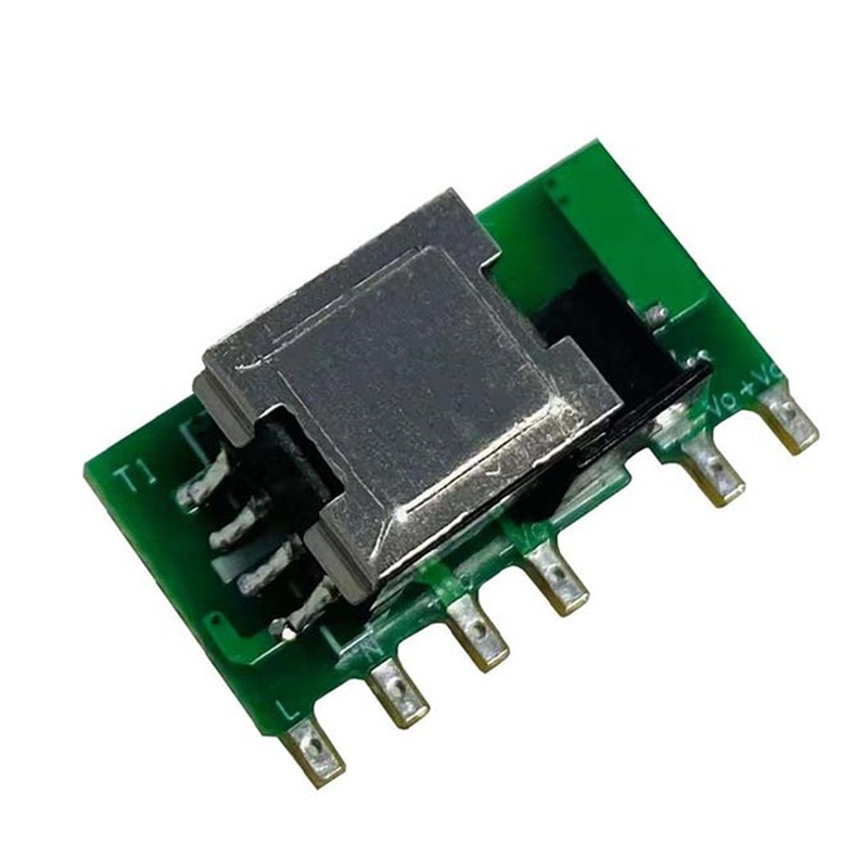
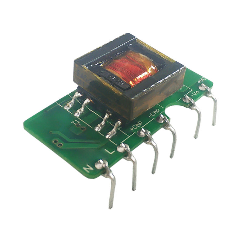
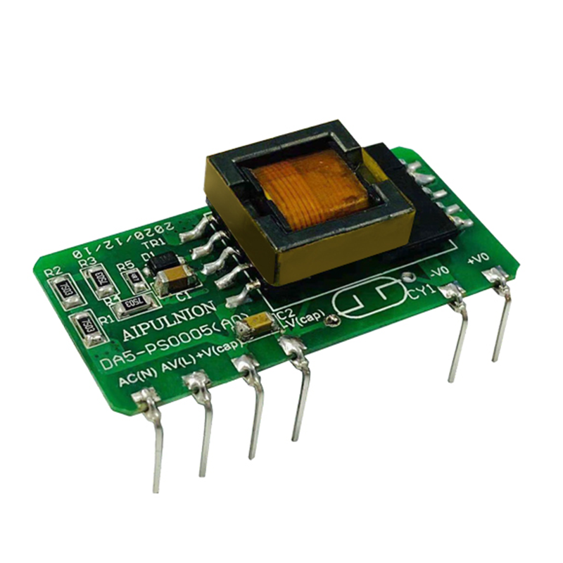
Post the PSFB magnetic device calculation method to share with everyone:
nOutput energy storage inductor design:
The output energy storage inductor of the phase-shifted full bridge can actually be regarded as a simple BUCK inductor. Since its positive and negative half cycles each work once, its operating frequency is equal to 2 times the switching frequency. Its calculation formula is:
Lf = Vo *(1-Dmin)/(4*fs* △I)
Lf in the above formula is the minimum inductance. The actual value should be greater than this value to ensure the continuity of the current. If the output voltage needs to be continuously adjustable within a certain range, then Vo should be Vo (min), that is
Lf = Vo(min) *(1-Dmin)/(4*fs* △I)
The above formula Dmin is for ease of understanding. In fact, the phase-shifted full-bridge duty cycle is constant, and there is no minimum duty cycle: that is
Dmin= Vo(min)/(Vin(max)/n-VLf-VD)
nMain transformer design:
First, calculate the minimum secondary output voltage of the phase-shifted full bridge:
Vsec(min)=(Vo(max)+VLf+VD)/ Dsec(max)
The primary and secondary transformer turns ratio is:
n=Vin(min) /Vsec(min)
To select the transformer, use the Ap method:
Ap =Ae*Aw= Po*104 /(4*ƞ*fs*△B*J*Ku*)
Next, calculate the number of primary turns of the transformer:
Np= Vin(min)*D(max)/(4*fs*Ae*Bmax)
Then the number of secondary winding turns is:
Ns= Np/n
nResonant inductor design:
The purpose of adding a resonant inductor is to achieve the ZVS of the lagging arm switching tube. As mentioned in the previous analysis, when the lagging arm resonates, the secondary inductance cannot be reflected to the primary through the transformer. In order to ensure the ZVS of the lagging arm switching tube, the energy of the resonant inductor must satisfy The following formula:
LrI2p/2=(V2in*C upper tube)/2+(V2in*C lower tube)/2= V2in*Clag
That is, Lr= 2* V2in*Clag /I2p
Where Lr: resonant inductance value
Vin: input voltage
Clag: Lagging arm capacitance (external capacitance and MOSFET junction capacitance)
Ip: the primary side current when the lagging bridge arm is turned off
The calculation also needs to consider the following factors:
Vin should take the highest input voltage value to ensure that the lagging bridge arm can achieve ZVS under any input voltage.
Considering that at light load Ipl (10%-20% load), the lagging bridge arm still needs to work in the ZVS state
When the output current iLf is at a certain value (such as 2A), the output energy storage inductor current is still continuous or at a critical point. That is to say, the pulsating current of the output energy storage inductor is equal to 2 times this value.
That is △ iLf = 2 *2A=4A
Then Ip=(Ipl+ △ iLf /2)/n