


Accurate calculation of switching power supply - how is the loop calculated?
Modular design switching power supply, comprehensive and accurate calculation of loop modules. Taking flyback as an example, mathcad software is used to comprehensively and accurately calculate the loop parameters to ensure 100% reliability.
To truly learn about power, you must learn mathematics well. Many people don't take it seriously, or they deliberately belittle it because they don't understand it. In fact, this is harmful. Mathematics is mainly divided into three directions, namely mathematical analysis, advanced algebra, and probability theory. The next step in mathematical analysis is the theory of functions of real variables, theory of functions of complex variables, and functional analysis. The next step up from advanced algebra is modern algebra. The next step in probability theory is mathematical analysis. The above mathematics are all the theoretical basis for learning power supply design. Even if you can't take a step closer for the time being, you must at least understand the first step in these three directions, namely mathematical analysis, advanced algebra, and probability theory.
Mathematical analysis, often referred to as calculus, is very useful for understanding power supply design. Specifically, it mainly focuses on understanding the time domain waveform of the circuit, especially solving ordinary differential equations and partial differential equations. Some students don’t understand it and even belittle it, which I personally feel is quite undesirable.
Real variable function theory is rarely used in power supplies, because in the design of switching power supplies, most functions are Riemannian integrable, that is, R integrable. There is no need to use Lebesgue integrability, that is, L is integrable. But there are no absolutes in everything. After all, real variable functions are a deepening of mathematical analysis. Riemannian integrability must be Lebesgue integrable, but not vice versa. Therefore, if you understand the real variable function theory, you can look at power supply design from a higher perspective. This is true for integrals, and of course it is also true for differentials.
Complex variable function theory is widely used in power supply design. Laplace transform and inverse transform are its most direct manifestations. It can be said that without complex variable function theory, there would be no design of switching power supply. In this post, the Laplace transform and the inverse transform are also used, because with this transform and the inverse transform, the loop calculation can be simplified. In circuit time domain calculations, because of the complex split domain characteristics of complex variable function theory, complex high-order operations can be converted into simple first-order linear operations, greatly simplifying calculations. At this point, most students should believe in the important role of advanced mathematics in power supply design. As for the idea that simple addition, subtraction, multiplication, division, square root and other elementary mathematics can suffice to design a switching power supply, this idea is wrong. If you don’t understand advanced mathematics, you think it is useless, you think that only elementary mathematics is enough, or you even think that advanced mathematics is just showing off and fooling you.
Functional analysis goes a step further and is not an analysis of logarithms, but an analysis of functions. The analysis of functions within the spatial scope greatly simplifies number operations. Reflected in many aspects of switching power supply design, such as Fourier decomposition, the calculation of the circuit, especially the filter, has been greatly simplified. It has also been very important in the loop calculation in this post, making the loop calculation of power supply design possible.
While advanced algebra mainly includes linear algebra, the loop calculations used in this article largely use matrix calculation methods in linear algebra. A brief explanation is to linearize the small signal of the nonlinear circuit to solve the reliability of its control.
The basic concepts in modern algebra, namely groups, rings, fields, lattice, and modules, are almost always used in the design of switching power supplies. General linear groups and special linear groups in matrices are examples of groups. Lattice is widely used in digital circuits, such as Boolean algebra. The method of using matrix operations to calculate loops in this post is an operation that belongs to the domain. Looking at the switching power supply with the concept of space, it can be considered as the application of modules. And in some cases, namely in broader and more general matrix operations, it is ring operations. It can be seen that modern algebra has raised the switching power supply to a higher level, allowing us to observe the essence and connotation of the switching power supply from a higher perspective.
Probability theory is closely related to the statistical laws of power supply, such as reliability and failure analysis, which allows designers to find the best compromise between cost and reliability, thereby maximizing profits.
Mathematical statistics deals with big data and plays an important role in the mass production of power supplies. For example, monitoring after the procurement of components. Generally, a certain number of sample spaces are sampled to reflect the overall confidence level, so that the reliability of mass production of power supplies can be ensured with the minimum cost.
Take the simplest flyback circuit as an example to calculate the loop of the power supply. Lifting the veil of loop design in power supply design: So loop calculation is so simple?
Follow the following three parts:
A. Small signal transfer function of the main circuit
A1. Power filter circuit
A2. Flyback circuit
B. Small signal transfer function of control circuit
B1. Proportional integral PI adjustment
B2, isolation optocoupler
B3, control chip
C. Total open-loop small signal transfer function
Part A Small signal transfer function of the main circuit
A1. Power filter circuit
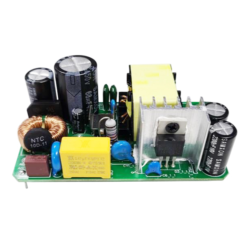
The first is the transfer function of the main circuit. The main circuit is divided into two parts. Let’s talk about the simple second part first, that is, the power filter circuit. It is mainly composed of the first-level output electrolytic capacitor, the output DC filter inductor, and the second-level output electrolytic capacitor, that is The so-called Π circuit.

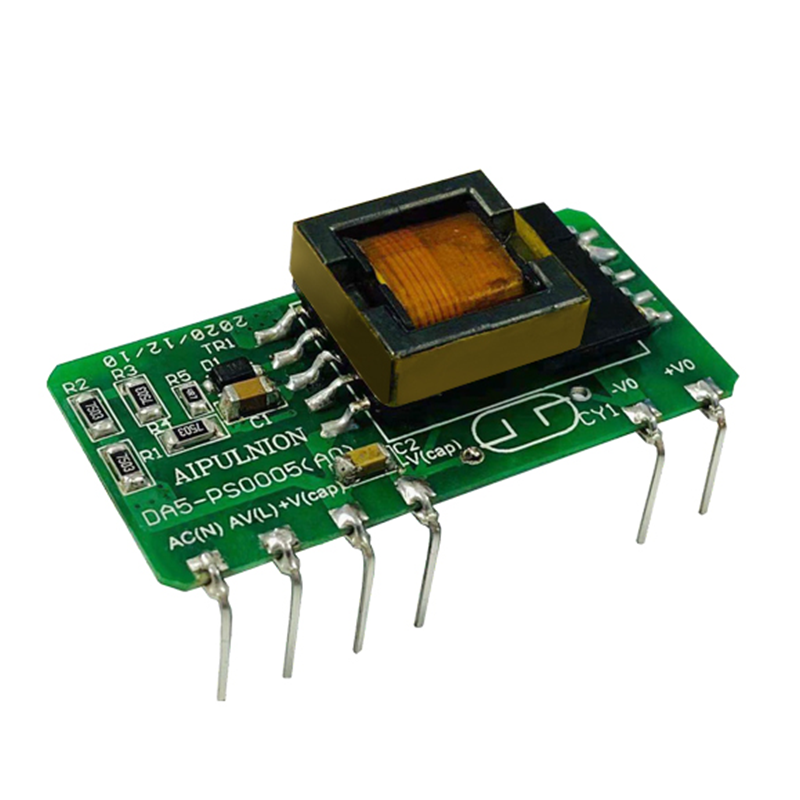
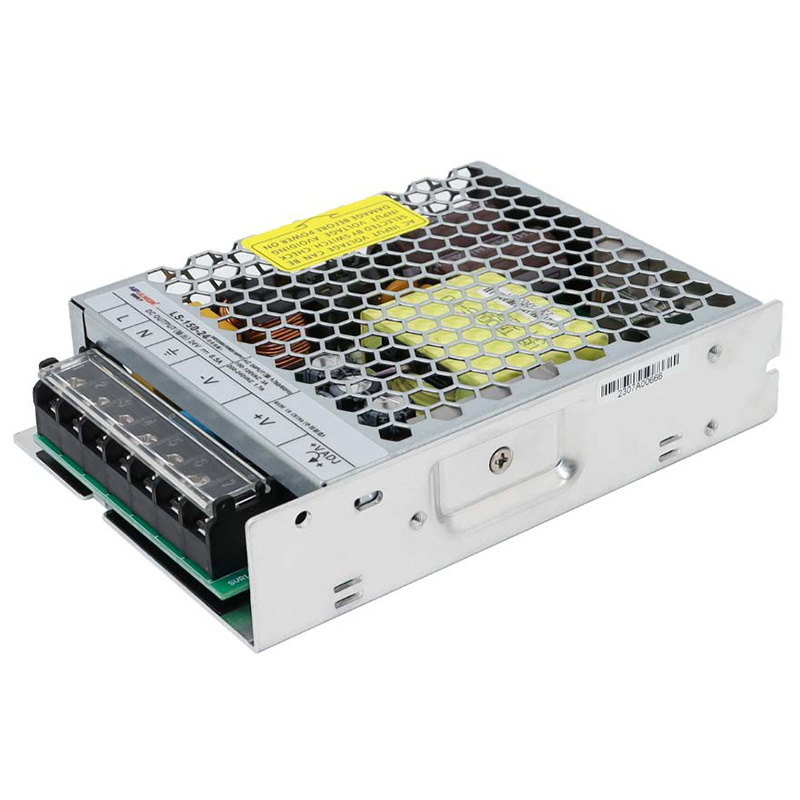
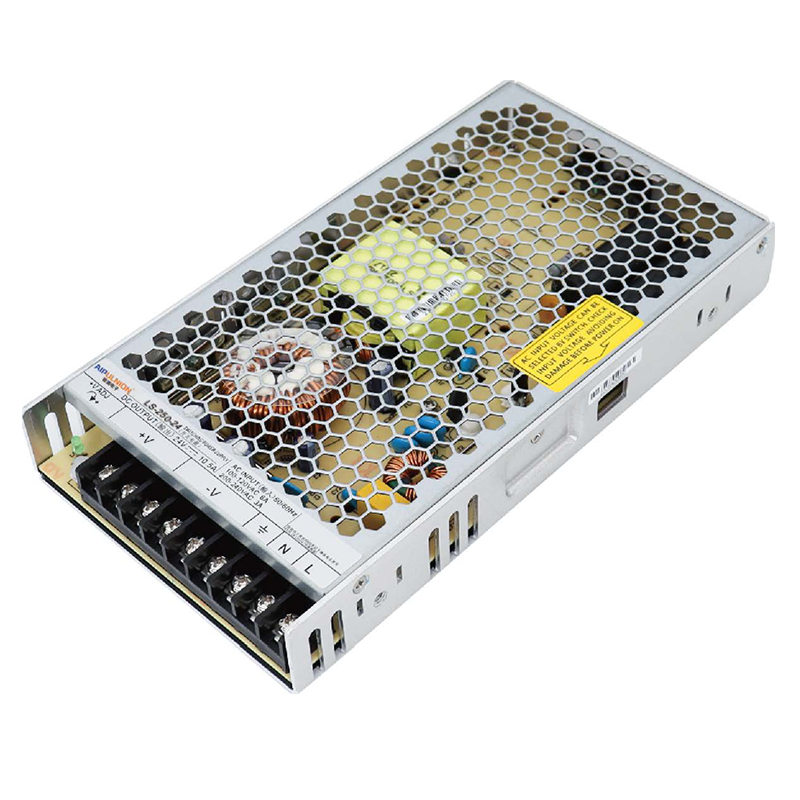
The circuit used is two outputs: 24V3.5A and 8V1.2A:

Some parameters of the main circuit are as follows:

The parameters of the first-stage output electrolytic capacitor, output DC filter inductor, and second-stage output electrolytic capacitor of the two outputs are as follows: The ESR of the electrolytic capacitor can be found according to the specification sheet of the electrolytic capacitor.
The schematic diagram of the filter circuit drawn by hand on the drawing board is as follows: Z1, Z2, and Z3 are as shown in the figure below.

This is the small signal transfer function of the filter circuit part of the main circuit. Since there is a 3-stage filter circuit before filtering and a 2-stage filter circuit after filtering, the difference is 1 stage filter circuit, that is, the slope decreases at -20dB per 10 times the frequency.


Power filter circuit amplitude-frequency phase-frequency curve
The voltage before filtering is the voltage on the first-stage electrolytic capacitor, and the voltage after filtering is the voltage on the second-stage electrolytic capacitor. Therefore, the small signal transfer function of the filter circuit is the ratio of the voltage after filtering to the voltage before filtering, which is also the voltage dividing ratio of the output filter circuit (that is, the equivalent output reactance of the third level is the equivalent output reactance of the second level = Zr3/ Zr2).
The block diagram of the small signal transfer function Gvv of the filter circuit part of the main circuit hand-drawn by the drawing board software is as follows, where Uo1 is the output voltage (before filtering) and Uo2 is the output voltage (after filtering):

Power filter circuit transmission block diagram
The corresponding power filter circuit diagram is as follows: where: Gvv=Uo2/Uo1

Power filter circuit
A2. Flyback circuit
These are some parameters of the small signal model of the flyback circuit with current peak control in the main circuit part 1. Of the 6 parameters, only 2 are actually required. The others are just listed and have no other meaning. Since the small signal models of the current continuous CCM and current discontinuous DCM modes are different, a piecewise function is used to unify them, and the software determines which mode to use. At the same time, judging from the final result, it is almost a smooth transition. Therefore, there will not be any reliability problems when the power supply switches between CCM and DCM (although many textbooks will say that DCM is easier to control than CCM, but this is not the case).

The above 6 parameters are all the small signal model that constitutes the peak control. The specific meaning is shown in the figure below. In the figure: vg is the input voltage, ig is the input current, v is the output voltage, R is the load resistance, and C is the filter capacitor (actually this should be the CLC filter circuit, that is, the first-stage output electrolytic capacitor, output DC filter inductor, Second-stage output electrolytic capacitor), due to the above reasons, v should be corrected to the output voltage before filtering.
ic is the current peak value (that is, the primary side current peak value in current peak control)
r1 is the input reactance, f1 is the input independent current source proportional coefficient (controlled by the current peak ic)
g1 is the input controlled current source admittance (controlled by the output voltage v)
r2 is the output reactance, f2 is the output independent current source proportional coefficient (controlled by the current peak ic)
g2 is the output controlled current source admittance (controlled by the output voltage v)

The following is the derivation of the core part of this article, which is the parameters of the small signal model of the flyback circuit.
The schematic diagram of the flyback converter is shown below:

The derivation is divided into 2 steps:
The first step is to derive the flyback small-signal model of average value control.
Step 2: Derive the flyback small-signal model of peak current control
The derivation steps are as follows:
1. First, derive the flyback small signal model of the average value controlled CCM mode;
2. Secondly, derive the flyback small-signal model (approximation) of the peak control CCM mode;
3. Derive the flyback small-signal model of peak control CCM mode again (accurate);
Fourth, derive the flyback small signal model of the average value controlled DCM mode again;
5. Finally, the flyback small-signal model (approximate) of the peak control DCM mode is derived
6. Finally, derive the flyback small signal model of the peak control DCM mode (accurate)
At the same time: the derivation is divided into two aspects:
A2.2.1 is the flyback small-signal model of continuous current mode CCM
A2.2.2 is the flyback small-signal model for discontinuous current mode DCM.
1. First, derive the flyback small signal model of the average value controlled CCM mode:
1. Average within one switching cycle
The D1 working area with duty cycle conduction is the working area where the switch Q1 is turned on and the diode D1 is turned off. The equivalent circuit is as shown in the figure below.
The state equation is:
L*di/dt=vg;
C*dv/dt=-v/R;
The output variables are:
ig=i;
v=v;

The D2 working area where the duty cycle is cut off is the working area where the switch Q1 is turned off and the diode D1 is turned on. The equivalent circuit is as shown in the figure below.
The state equation is:
L*di/dt=-v/n;
C*dv/dt=i/n-v/R;
The output variables are:
ig=0;
v=v;

The small signal model is: averaging over a switching cycle. Therefore, the following equation can be derived from the equations of the above two working areas by taking the average (that is, multiplying the duty cycle *d1, *d2 respectively, and then adding +):
The state equation is:
L*di/dt=d1*vg+d2*(-v/n);
C*dv/dt=d1*(-v/R)+d2*(i/n-v/R);
The output variables are:
ig=d1*i+d2*0;
v=d1*v+d2*v;
Since it is current continuous mode CCM, the conditions are met:
d1+d2=1;
So, simplify it:
The state equation is:
L*di/dt=d1*vg+d2*(-v/n);
C*dv/dt=-v/R+d2*i/n;
The output variables are:
ig=d1*i;
v=v;
2. Separate AC small signal equations
Method 1:
Write each variable as the sum of the DC large signal component and the AC small signal component, that is:
i=I+i~;
v=V+v~;
vg=Vg+vg~;
ig=Ig+ig~;
d1=D1+d~;
d2=D2-d~;
in
D1+D2=1;
Substituting the above variables into the above equation, we can get:
The state equation is:
L*d(I+i~)/dt=(D1+d~)*(Vg+vg~)+(D2-d~)*(-(V+v~)/n);
C*d(V+v~)/dt=-(V+v~)/R+(D2-d~)*(I+i~)/n;
The output variables are:
(Ig+ig~)=(D1+d~)*(I+i~);
(V+v~)=(V+v~);
Method 2:
In fact, there is a simpler way to find its DC large signal equation and AC small signal equation, namely:
① DC large signal equation: It can be obtained by directly replacing the variable x with the DC quantity X. Since dX/dt=0, then:
The state equation is:
0=D1*Vg+D2*(-V/n);
0=-V/R+D2*I/n;
The output variables are:
Ig=D1*I;
V=V;
The supplementary equation is:
D1+D2=1;
② AC small signal equation: If x~ is regarded as partial differential dx, then since d(x*y)=(X*dy+Y*dx), so (x*y)~=(X*y~+Y *x~), then differentiating both the left and right sides of the equation simultaneously can be obtained:
The state equation is:
L*di~/dt=(D1*vg~+Vg*d1~)+(D2*(-v~/n)+(-V/n)*d2~);
C*dv~/dt=(-v~/R)+(D2*i~/n+I/n*d2);
The output variables are:
ig~=(D1*i~+I*d1~);
v~=(v~);
The supplementary equation is:
d1~+d2=0;
Simplified to:
The state equation is:
L*di~/dt=D1*vg~+(Vg+V/n)*d~-D2/n*v~;
C*dv~/dt=-1/R*v~+D2/n*i~-I/n*d~;
The output variables are:
ig~=D1*i~+I*d~;
v~=v~;
Simplified, it looks like this:
The state equation is:
L*di~/dt=[D1*Vg-D2*V/n]+[D1*vg~+(Vg+V/n)*d~-D2/n*v~]+[d~*vg~ +d~*v~/n];
C*dv~/dt=[-V/R+D2*I/n]+[-1/R*v~+D2/n*i~-I/n*d~]+[-d~*i ~/n];
The output variables are:
Ig+ig~=[D1*I]+[D1*i~+I*d~]+[d~*i~];
V+v~=[V]+[v~];
So the DC large signal equation is:
The state equation is:
0=D1*Vg-D2*V/n;
0=-V/R+D2*I/n;
The output variables are:
Ig=D1*I;
V=V;
Ignoring the second-order small signal, the AC small signal equation is:
The state equation is:
L*di~/dt=D1*vg~+(Vg+V/n)*d~-D2/n*v~;
C*dv~/dt=-1/R*v~+D2/n*i~-I/n*d~;
The output variables are:
ig~=D1*i~+I*d~;
v~=v~;
3. Laplace L transform, simplifying the AC small signal equation
Transform the above AC small signal equation into Laplace transform, that is, transform from time domain t to frequency domain s: therefore di~/dt is transformed into s*i~, and dv~/dt is transformed into s*v~; where s=j *ω=j*2*π*f; (where ω is the angular frequency, π=3.14, and f is the frequency).
The state equation transforms into:
L*s*i~=D1*vg~+(Vg+V/n)*d~-D2/n*v~;
C*s*v~=-1/R*v~+D2/n*i~-I/n*d~;
The output variable is transformed into:
ig~=D1*i~+I*d~;
v~=v~;
The AC small signal equation after the above transformation Eliminate i~ and simplify to get:
ig~=1/Δ*[(n*D1/D2)^2*((1+R*C*s)/R)*vg~+(n^2*D*Vg/(D2^3*R )*(Δ+(1+R*C*s)*(1-Ln*D1/R*s))*d~];
v~=1/Δ*[n*D1/D2*vg~+n*Vg/D2^2*(1-Ln*D1/R*s)*d~];
in:
Ln=(n/D2)^2*L;
Δ=1+Ln/R*s+Ln*C*s^2;
4. The equation controlled by the average value is represented by a circuit diagram model
Then the CCM small signal model controlled by the average value is shown in the figure below:
According to the figure below, we can know:
ig~=1/Z*vg~+(j+e/Z)*d~;
v~=M*He*vg~+e*M*He*d~;
Corresponding the above formula to the corresponding terms in the AC small signal equation after transformation and simplification, we can get:
M=V/Vg=n*D1/D2; (according to the state equation in the above DC large signal equation)
He=1/Δ;
Le=Ln=(n/D2)^2*L;
Ce=C;
e=V/(n*D1^2)*(1-Ln*D1/R*s);
j=n/D2^2*V/R;
Pictures are loading...
2. Secondly, derive the flyback small-signal model (approximation) of the peak control CCM mode.
5. Establish a supplementary equation for the peak current ic~ and simplify the AC small signal equation
The AC small signal equation after the Laplace transform of the above average value controlled CCM mode is re-listed as follows:
The state equation transforms into:
L*s*i~=D1*vg~+(Vg+V/n)*d~-D2/n*v~;
C*s*v~=-1/R*v~+D2/n*i~-I/n*d~;
The output variable is transformed into:
ig~=D1*i~+I*d~;
v~=v~;
Assuming that the CCM mode inductor average current i is approximately equal to the inductor peak current ic, as shown in the figure below, then:
ic~=i~;
Pictures are loading...
Eliminate i~ and d~ from the AC small signal equation after the above transformation, and after simplification we can get:
ig~=D1*(1+n*S*L/R)*ic~+D1*D2/R*v~-n*D1^2/R*vg~;
S*C*v~=D2/n*(1-n*S*L*D1/(D2*R))*ic~-(1/R+D1*D2/(n*R))*v~ +D1^2/R*vg~;
6. The equation of peak value control is represented by a circuit diagram model.
Then the CCM small signal model of peak control is shown in the figure below:
According to the figure below, we can know:
ig~=f1*ic~+g1*v~+1/r1*vg~;
S*C*v~=f2*ic~-(1/R+1/r2)*v~+g2*vg~;
Corresponding to the corresponding terms in the AC small signal equation after transformation and simplification, we can get: (approximately)
f1=D1*(1+n*S*L/R);
g1=D1*D2/R;
r1=-R/(n*D1^2);
f2=D2/n*(1-n*S*L*D1/(D2*R));
r2=n*R/(D1*D2);
g2=D1^2/R;
Pictures are loading...
3. Derive the flyback small-signal model of the peak control CCM mode again (accurate):
5. Establish a supplementary equation for the peak current ic~ and simplify the AC small signal equation
Method 1:
As shown in the figure below: In the two working areas of D1 and D2, the difference between the average i and the peak ic is m1*d1*Ts/2 and m2*d2*Ts/2 respectively, then the difference is d1*m1* d1*Ts/2+d2*m2*d2*Ts/2. but:
i=ic-m1*d1^2*Ts/2-m2*d2^2*Ts/2;
in:
d1+d2=1;
Write each variable as the sum of the DC large signal component and the AC small signal component, that is:
i=I+i~;
ic=Ic+ic~;
m1=M1+m1~;
m2=M2+m2~;
d1=D1+d~;
d2=D2-d~;
in:
D1+D2=1;
but:
(I+i~)=(Ic+ic~)-(M1+m1~)*(D1+d~)^2*Ts/2-(M2+m2~)*(D2-d~)^2* Ts/2;
Ignoring the second and third order small signals, the AC small signal equation is:
i~=ic~-(M1*D1-M2*D2)*Ts*d~-D1^2*Ts/2*m1~-D2^2*Ts/2*m2~;
Since M1*D1=M2*D2, it can be simplified to:
i~=ic~-D1^2*Ts/2*m1~-D2^2*Ts/2*m2~;
in:
m1~=vg~/L;
m2~=v~/(n*L);

The AC small signal equation after the Laplace transform of the above average value controlled CCM mode is re-listed as follows:
The state equation transforms into:
L*s*i~=D1*vg~+(Vg+V/n)*d~-D2/n*v~;
C*s*v~=-1/R*v~+D2/n*i~-I/n*d~;
The output variable is transformed into:
ig~=D1*i~+I*d~;
v~=v~;
At the same time, it can be derived from the above:
i~=ic~-D1^2*Ts/2*m1~-D2^2*Ts/2*m2~;
in:
m1~=vg~/L;
m2~=v~/(n*L);
Eliminate i~ and d~ from the AC small signal equation after the above transformation, and after simplification we can get:
ig~=D1*(1+n^2*S*L/(D2*R))*ic~+(n*D1/R-D1*D2^2*Ts/(2*L*n)-S *n*D1*D2*Ts/(2*R))*v~-(n^2*D1^2/(D2*R)+D1^3*Ts/(2*L)+S*n^ 2*D1^3*Ts/(2*D2*R))*vg~;
S*C*v~=D2/n*(1-n^2*D1*S*L/(D2^2*R))*ic~-(1/R+D1/R+D2^3*Ts /(2*L*n^2)-D1*D2*S*Ts/(2*R))*v~+(n*D1^2/(D2*R)-D1^2*D2*Ts/ (2*L*n)+S*n*D1^3*Ts/(2*D2*R))*vg~;
Method 2:
In fact, there is also a simpler way to find the equation of ic~. If x~ is regarded as a partial differential dx, then since d(x*y^2)=(X*2*Y*dy+Y^2* dx), so (x*y^2)~=(X*2*Y*y~+Y^2*x~), then differentiate the left and right sides of the equation at the same time:
i~=ic~-(M1*2*D1*d1~+D1^2*m1~)*Ts/2-(M2*2*D2*d2~+D2^2*m2~)*Ts/2;
d1~+d2~=0;
Since M1*D1=M2*D2, it can be simplified to:
i~=ic~-D1^2*Ts/2*m1~-D2^2*Ts/2*m2~;
in:
m1~=vg~/L;
m2~=v~/(n*L);
6. The equation of peak value control is represented by a circuit diagram model.
Then the CCM small signal model of peak control is shown in the figure below:
According to the figure below, we can know:
ig~=f1*ic~+g1*v~+1/r1*vg~;
S*C*v~=f2*ic~-(1/R+1/r2)*v~+g2*vg~;
Corresponding to the corresponding terms in the AC small signal equation after transformation and simplification, we can get: (accurate)
f1=D1*(1+n^2*S*L/(D2*R));
g1=n*D1/R-D1*D2^2*Ts/(2*L*n)-S*n*D1*D2*Ts/(2*R); D1^2/(D2*R)+D1^3*Ts/(2*L)+S*n^2*D1^3*Ts/(2*D2*R));
f2=D2/n*(1-n^2*D1*S*L/(D2^2*R));
r2=1/(D1/R+D2^3*Ts/(2*L*n^2)-D1*D2*S*Ts/(2*R));
g2=n*D1^2/(D2*R)-D1^2*D2*Ts/(2*L*n)+S*n*D1^3*Ts/(2*D2*R);

4. Derive the flyback small-signal model of the average value controlled DCM mode again.
1. Average within one switching cycle
The equivalent circuits of the D1 and D2 working areas are the same as those in the average value control CCM mode, so they will not be repeated here. For details, see posts 226 and 228.
The D3 working area where the duty cycle is cut off is the working area where the switch Q1 is turned off and the diode D1 is turned off. The equivalent circuit is as shown in the figure below.
The state equation is:
L*di/dt=0;
C*dv/dt=-v/R;
The output variables are:
ig=0;
v=v;

Trail:
1. Crossover frequency (fc) ωc:
The frequency value corresponding to when the open-loop logarithmic amplitude-frequency characteristic is equal to 0dB is called the open-loop crossover frequency or cut-off frequency ωc. It represents the fast performance of system response. The larger the value, the better the fast performance of the system. In order to prevent the step response from overshooting, the crossover frequency ωc should be located on a line segment with a slope of -20dB/dec. If the slope of the mid-frequency band is -20dB/dec, the system must be stable.
2. Phase margin φm:
φ is defined as the difference between the phase value φ(ωc) and -180 degrees of the open-loop logarithmic frequency characteristic phase-frequency characteristic curve when ω=ωc, that is, φm(ωc)=φ(ωc)+180 degrees. The physical meaning of phase margin φm (ωc): In order to maintain system stability, the maximum phase lag allowed to be added to the open-loop frequency characteristics of the system when ω = ωc. If φm(ωc)>0, the system is stable; if φm(ωc)=0, the system is critically stable; if φm(ωc)<0, the system is unstable. For an automatic control system, it is generally believed in the engineering field that φm(ωc)=45 degrees, indicating sufficient phase margin in the local system.
3. Gain margin Kg:
The gain margin Kg refers to the number of decibels corresponding to the reciprocal amplitude when the phase angle ωg=180 degrees, that is, Kg=20*log(1/|T(j*ωg)|)=-20*log|T( j*ωg)| (dB); The physical meaning of gain margin Kg: in order to maintain system stability, the maximum number of decibels allowed to be increased in the open-loop gain of the system. If Kg>0, the system is stable; Kg=0, the system is critically stable; Kg<0, the system is unstable. For an automatic control system, it is generally believed in the engineering field that Kg>10dB, the system has sufficient amplitude margin.
4. IF width h:
The width of the open-loop logarithmic amplitude-frequency characteristic that crosses the horizontal axis with a slope of -20dB/dec on the ω axis is called the intermediate frequency width (or intermediate frequency bandwidth), that is, h=ω2/ω1; the intermediate frequency bandwidth reflects the system The greater the stability of h, the greater the phase angle margin of the system. In order to obtain better transient response performance indicators, the IF width should be greater than the specified value. The larger the IF width, the closer the step response curve is to the exponential curve. If the step response curve of a system is closer to an exponential curve, the crossover frequency ωc is inversely proportional to the time constant of the exponential curve. However, the larger the intermediate frequency bandwidth h is, the larger the high-frequency noise will be.